Fabrication of Micro-Contact Probe Using Mo-Cr Spring with Au Plating Bump
- PDF / 101,261 Bytes
- 5 Pages / 612 x 792 pts (letter) Page_size
- 46 Downloads / 252 Views
A5.12.1
Fabrication of Micro-Contact Probe Using Mo-Cr Spring with Au Plating Bump
Chinami Kaneshiro and Kohji Hohkawa Electric & Electrical Engineering, Kanagawa Institute of Technology 1030 Shimo-Ogino, Atsugi-shi, Kanagawa 243-0292, JAPAN
ABSTRACT In this paper, we report a new technology for fabricating interconnects and/or contact probes for LSI fabrication. We used a Mo-Cr spring wire as a lead wire. To reduce the resistance of the lead wire, we applied a Au plating bump to the tip of a Mo-Cr spring covered with Au thin film. Experimental results showed that contact resistance was lowered by forming an Au plating bump on the Mo-Cr spring wire, which was plated under controlled conditions.
INTRODUCTION The electrode-pads on integrated circuit chips are increasingly high density and small size. However, in IC chips, the electrode pads and metal wires occupy a large proportion of the area. In using micro-probes for wafer testing, it is necessary to establish a fine alignment between the probe arrays and the electrode pads in the ICs. A metal probe array has been proposed as a new technique for use in interconnect and probe technology [1-5]. In particular, micro-spring technology has potential applications in both these technologies [3-5]. The key issues in interconnect technology are as follows: (1) resistance of probes connecting devices, and (2) interaction of microwaves in high-frequency fields. The main problems in probe technology are contact resistance between probes and electrode pads, and mechanical damage to probes due to repeated wafer testing. A common problem is resistance in microprobes. Therefore, to address these issues, we propose novel contact probes that consist of spring fingers. We also focused on reducing contact resistance between the electrode pads and microprobes. In this paper, we present the results of a basic study on the fabrication of a micro-spring contact probe with an Au plating bump. We also discuss the use of sputter-deposition to fabricate the micro-spring contact probes and examine contact resistance in Au electrode pads in relation to using Au plating bumps to reduce contact resistance.
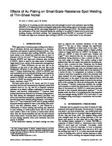
MICRO-CONTACT PROBING TECHNOLOGY Even though devices are becoming smaller, the area occupied by the pad and wiring is still significant. The problem with interconnect and/or probing technology in ICs is contact resistance between the electrode pads in devices and contact probes. Figure 1 shows a schematic illustration of our proposed micro-contact probe with an Au
A5.12.2
For interconnection optics for AFM electric for STM or micro-probe
(a)
For micro-probe Fig. 1 Schematic illustrations of proposed contact probe. (a) spring array, and (b) applications of the array in interconnects and probing methods. bump for interconnect and probing technology. The wire spring is made of elastic metal materials, e.g., Mo-Cr. Spring wire is used for interconnects in three-dimensional wiring as well as for probes in scanning probing microscopy and wafer probing. The advantage of using wire springs in
Data Loading...