Highly Reliable Metal Gate nMOSFETs by Improved CVD-WSix films with Work Function of 4.3eV
- PDF / 345,394 Bytes
- 6 Pages / 595 x 842 pts (A4) Page_size
- 8 Downloads / 383 Views
D4.2.1
Highly Reliable Metal Gate nMOSFETs by Improved CVD-WSix films with Work Function of 4.3eV Kazuaki NAKAJIMA, Hiroshi NAKAZAWA, Katsuyuki SEKINE, Kouji MATSUO, Tomohiro SAITO, Tomio KATATA, Kyoichi SUGURO and Yoshitaka TSUNASHIMA Process and Manufacturing Engineering Center, Semiconductor Company, Toshiba Corporation, 8, Shinsugita-cho, Isogo-ku, Yokohama 235-8522, Japan Phone/Fax: +81-45-770-3662/3577, e-mail: [email protected] ABSTRACT In this paper, we first propose an improved CVD-WSix metal gate suitable for use with nMOSFETs. Work function of CVD-WSi3.9 gate estimated from C-V measurements was 4.3eV. The nMOSFET using CVD-WSi3.9 gate electrode showed that Vth variation of L/W=1µm/10µm nMOSFETs can be suppressed to be lower than 8mV in 22chip. In CVD-WSi3.9 gate MOSFETs with gate length of 50nm, a drive current of 636µA/µm was achieved for off-state leakage current of 35nA/µm at 1.0V of power supply voltage. By using CVD-WSi3.9 gate electrode, highly reliable metal gate nMOSFETs can be realized. INTRODUCTION Poly-Si gate depletion is an important issue in 65nm technology node and beyond, since the gate depletion causes the increase of total effective oxide thickness. Metal gate electrode is more advantageous than poly-Si gate electrode because there is no gate depletion region. We reported that process damage to gate oxide must be suppressed during deposition of TiN metal gate and CVD process is needed to realize metal gate transistors [1-2]. However, it is difficult to realize lower Vth metal gate transistors using TiN metal gate having work function of midgap. Recently, many researchers have reported on dual metal gate electrode. Since work function of metal gate depends on material, two materials are needed for metal gate having optimized work function for nMOS and pMOS FETs[3-5]. In this paper, we first propose an improved CVD-WSix metal gate with work function of 4.3eV as gate electrode for nMOSFETs and discuss the relationship between the Si/W ratio of CVD-WSix and electrical properties of MOSFETs.
D4.2.2
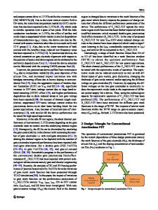
EXPERIMENTAL In this study, we fabricated CVD-WSi3.9 gate transistors by damascene gate process. Because, CVD-WSi gate electrode can not be thermally stable up to 800C thermal processing. Figure 1 show the process flow of damascene gate process. A dummy gate, composed of polySi, is isotropically etched by dry etching in order to make narrow gate grooves. Source and drain were formed after sidewall formation. After deposition and planarization of pre-metal dielectric film, the dummy gate was removed by plasma etching in order to make narrow gate grooves. After dummy gate removal, ion implantations were carried out through the gate groove in order to make local channel profile for adjusting threshold voltage of transistors. Activation annealing was carried out by spike RTA at 1000C. Plasma SiON and CVD-WSix film are used for gate insulator and gate electrode, respectively. A Si/W ratio of CVD-WSix films was changed from 2.4 to 3.9 by controlling tungsten hexafluoride (WF6) and dichl
Data Loading...