Localized or Delocalized Electrons in Microcrystalline Silicon?
- PDF / 414,646 Bytes
- 6 Pages / 414.72 x 648 pts Page_size
- 56 Downloads / 469 Views
x 10
0
II
20 K 20KO
"104
............... .... ................................... I * 333I
"-17ppm CO
U)10
-........
I.IW
0
"••............... ...................... .
o 133
..... ...........
---
/
C-
Cr
v'66 .
7•'
AHFS =110 G 1 02 ------------------------------------
50 G
0 10
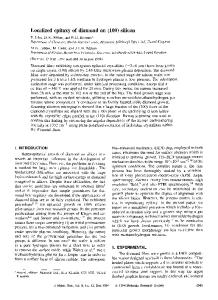
Fig. 1: Dark ESR spectrum of sample 17 at 20 K. The magnified curve shows a hyperfine doublet with a splitting of 110 G.
T(K)
100
Fig. 2: ESR signal intensity of the CE line as a function of temperature for samples 1, 33, 67 and 133. The solid line of slope -1 represents the Curie law ( o 1/T).
RESULTS In the following the samples are denoted by their gas phase doping ratio, e.g. sample 17 corresponds to the sample with a gas phase doping level of 17 ppm. In Fig. 1 the ESR signal of sample 17 is shown. The CE signal at g=1.998 is the dominating feature. Upscaling the signal, the hyperfine (hf) doublet due to phosphorus atoms becomes visible at low temperatures (< 70 K). The hyperfine splitting AHFS is 110 G, which is between the values reported for crystalline (42 G) and amorphous silicon (245 G)[4]. The hyperfine lines only appear as shoulders in the broad wings of the Lorentzian-type center line. The intensity of the hyperfine doublet at 20 K is less than 5% of the overall signal intensity. No hyperfine lines appear in the lightly doped samples and in samples with higher doping the hyperfine signal was again weaker. The temperature dependence of the CE signal intensity is shown in a double-logarithmic plot in Fig. 2 for samples 1, 33, 67 and 133. For comparison the intensities have been normalized to the same value at low temperature. The solid line indicates the temperature dependence which would be expected from the Curie law (prop. f/T). Generally the data of all samples follow this dependency. For samples 33 and 67 a deviation is observed at high temperatures. Fig. 3 shows the dark conductivities Od of samples 1, 17, 33 and 67 versus 1000/T. We find the characteristic temperature dependence of a for jtc-Si:H which is indicative of a distribution of activation energies [5]. To estimate the activation energies involved in the conduction process at low temperatures we approximate the Od-vs.-T plots by straight lines in the temperature region below T = 20 K. The slope of these lines corresponds to an activation energy of 4 meV for samples 17, 33 and 67. Fig. 4 shows a plot of the dark conductivity at various temperatures between 40 K and 300 K versus the spin density (NcE) of the CE line at 40 K. The dashed line corresponds to the curve of slope 1, where a would be proportional to NCE. The ad-vs.-NCE-curves approach a linear relation with increasing measurement temperature for the conductivity. 752
10-2 E 10-4 03 10.6 Cn 10.8 10-1010-12
0
50
100
150
200
250
1000ff (K1) Fig. 3: Dark conductivities for samples 1, 17, 33 and 67 as a function of the inverse of temperature. The lines are approximations to the experimental data for an estimate of the dominant activation energies.
1 E 10 10-6
10.8
NCE at 40K
Data Loading...