In Situ Stem Technique for Characterization of Nanoscale Interconnects During Electromigration Testing
- PDF / 2,176,309 Bytes
- 6 Pages / 417.6 x 639 pts Page_size
- 63 Downloads / 383 Views
OF
NANOSCALE
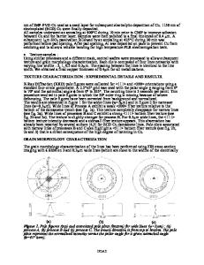
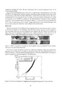
Ismail Gobulukoglu and Brian W. Robertson Department of Mechanical Engineering and the Center for Materials Research and Analysis University of Nebraska, Lincoln, Nebraska 68588-0656 Abstract A technique for observing microstructure and morphology changes during annealing or electromigration of 100 nm-scale and smaller interconnects is presented. The technique is based on dynamic in situ characterization using a UHV field-emission scanning transmission electron microscope (STEM) and can enable full microstructural characterization (images, diffraction patterns and compositions) during electromigration testing. Initial steps in the validation of the approach include in situ electron-beam OMCVD of Al-containing wires and observation of these wires. Although the deposition conditions were not optimized, Al-containing wires, with high edge acuity, thickness uniformity, and with minimum interconnect widths as small as 15 nm have successfully been deposited. In situ imaging of the annealing of 100 nm Al films on 25 nm Si3N 4 substrates at 350 'C demonstrates that an image resolution of 10 nm should readily be attainable in passivated nanoscale interconnects during electromigration. Introduction Direct observation has given dynamic information on electromigration damage in micronscale or wider interconnects for the past 30 years. A number of tools have been employed for in situ electromigration observation of interconnects. These include scanning electron microscopy (SEM) [1,2,3], transmission electron microscopy (TEM) [4,5,6,7], atomic force microscopy
(AFM) [8], focussed ion beam (FIB) [9], t-reflection high energy electron diffraction microscopy ([t-RHEED) [10], and microbeam x-ray diffraction (MXRD) [11 ]. More complete dynamic real time characterization of interconnects is key to understanding the fundamental mechanisms present during electromigration. However, this generally becomes more difficult to achieve as the interconnect widths scale down much below 1 micron. A side view transmission method of sufficient resolution and yielding sufficient signal is required. Here, we propose a side view approach that will enable researchers to obtain quite complete information on changes in microstructure of interconnects during electromigration. At the deep submicron scale, there are few tools that can provide characterization of one or more aspects of the surface and internal structure of interconnects encapsulated in dielectric. The choice of tool must enable strain and other information to be acquired from very small regions - 10 nm or less in the case of 100 to 200 nm wide interconnects. This limits the choice to field emission STEM, field emission (S)TEM, or, perhaps in future, a form of x-ray nanodiffraction / imaging. Of these, field emission STEM methods are the most applicable. We therefore propose UHV field emission STEM as a primary tool for in situ investigation during electromigration testing. The UHV field emission STEM is designed for optimum use of a small probe to analyze different regions wi
Data Loading...