Integration and Performance Improvements of Silicon Nanocrystal Memories
- PDF / 344,958 Bytes
- 8 Pages / 595 x 842 pts (A4) Page_size
- 18 Downloads / 303 Views
D1.5.1
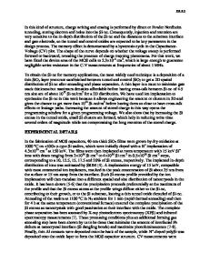
Integration and Performance Improvements of Silicon Nanocrystal Memories T. Hiramoto, I. Kim, M. Saitoh, and K. Yanagidaira Institute of Industrial Science, University of Tokyo 4-6-1 Komaba, Meguro-ku, Tokyo 153-8505, Japan ABSTRACT The silicon nanocrystal memory, that is one of the most promising devices for future non-volatile memory, is extensively investigated by experiments and simulation. The silicon nanocrystal memory cells are successfully integrated using the state-of-the-art 0.13 µm DRAM technology. The mechanism of the two-bit-per-cell operation, that is one of the unique features of silicon nanocrystal memory, is investigated and it is shown that the degree of DIBL determines the read scheme of the two-bit-per-cell operation. Moreover, the dependences of memory characteristics on device structures are examined by fabrication and measurements and it is found that the ultra-thin-body SOI and double-gate structures have better memory characteristics. INTRODUCTION Silicon nanocrystal memories, where silicon nanocrystals are embedded in gate oxide and act as storage nodes, have attracted much attention [1,2]. Physical separation of nanocrystals makes it possible to improve the endurance and reliability of cell operation, and it is well recognized that silicon nanocrystal memory will be promising for future non-volatile, high-density memory that can replace conventional floating gate memories. Although many research works have been reported previously on silicon nanocrystal memory, much more improvements of integration level, performance, and reliability will be achieved by proper optimizations of process and device structures. In this paper, we report (1) full process integration of silicon nanocrystal memory cells using advanced memory technology, (2) the mechanism of two-bit-per-cell operation that is a unique feature of silicon nanocrystal memory, and (3) performance improvements of memory characteristics using ultra-small nano-scale SOI channel. INTEGRATION OF SILICON NANOCRYSTAL MEMORY So far, there have been some reports on design schemes of NCM for high density integration [3,4], but it is impossible to go beyond its scaling limitation without highly scalable process. In general, the cell area is determined by wordline (WL) and bitline (BL) pitches, and BL contact size. Fig. 1 shows the cell structure we proposed [5]. Landing plug polysilicon contact (LPC) and direct tungsten BL can enhance the integrated density thanks to self-aligned contact (SAC) and chemical mechanical polishing (CMP). Using these techniques, silicon nanocrystal memory cells with 4.6 F2 cell size on NOR type are successfully integrated. The cell size is 0.077 µm2 using the 130 nm memory technology.
D1.5.2
IDS(A)
(a) (b) Figure 1. (a) Schematic bird’s view of a fabricated silicon nanocrystal memory cell. (b) A cell layout of a silicon nanocrystal memory cell.
10
-5
10
-6
10
-7
10
-8
10
-9
10
-10
10
-11
10
-12
10
-13
0 1 2 w/o NCs
-1
VGS(V)_w/o NCs 3 4 5 6
Virgin
7
8
Write(S+D) Write(S) Write(D)
Data Loading...