Integration of Low Dielectric Constant Materials in Advanced Aluminum and Copper Interconnects
- PDF / 3,047,042 Bytes
- 13 Pages / 417.6 x 639 pts Page_size
- 95 Downloads / 379 Views
typically accomplished by reducing interconnect metal pitch and/or adding more interconnect metal layers. However, a reduction in metal pitch leads to increased interconnect parasitic; i.e., both interconnect capacitance and resistance are increased. Adding more interconnect metal layers leads to yield loss and higher manufacturing costs. To lessen these difficulties and challenges, advanced interconnect systems using new materials and new integration architectures are in demand for current and future ULSI circuits [1,2]. In comparison to the traditionally used interconnect materials, i.e., SiO 2 and Al, using low dielectric constant (low-K) materials as intralevel and/or inter-level dielectric (ILD) and high conductive metals, such as Cu, as wiring material not only can decrease the interconnect parasitics but also can reduce the number of metal layers for a required interconnect density [3-5]. There are generally two schemes to integrate low-K materials in interconnect structures fabricated either by a conventional subtractive-etch process or by a damascene process. In the first scheme, IOW-K materials are used as both the intra-level and the inter-level dielectric in conjunction with thin cap/hardmask layers (if necessary for processing). In the second scheme, low-Kc materials are used only as the intra-level dielectric (i.e., the dielectric between the metal lines) and conventional SiO 2 is used as the inter-level dielectric (i.e., the dielectric between the metal
485 Mat. Res. Soc. Symp. Proc. Vol. 564 ©1999 Materials Research Society
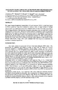
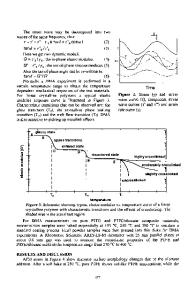
layers). Using the second low-K integration scheme can alleviate many processing issues related to low-K materials and improve the mechanical strength and heat dissipation of the interconnect structures [6,7]. However, the interconnect capacitance improvement in the second scheme is limited in comparison to the first scheme. Fig. 1 and Fig. 2 show calculated interconnect wiring capacitance as a function of metal linewidth/space for low-K (K = 2) interconnects of the first scheme (homogeneous low-K) and the second scheme (embedded low-K) and they are compared to the interconnects with SiO 2 (K = 4) ILD. Fig. I shows a scaling scenario where the vertical dimensions (metal height and space between the metal layers) are kept constant and only horizontal dimensions (metal linewidth and space) are scaled. The shaded area in Fig. 2 corresponds to a scaling scenario where the vertical dimensions of the interconnect structures are scaled by the same factor as the horizontal dimensions. In this case, the metal line aspect ratio (AR) is a constant as the interconnect linewidth/space is reduced.
nH40
P 1'0
11 11
Fixed Vertical Dimension 0.60-
0.60
E 0.50U-L
a) (. (U
0.40* 0.30*
--- Si02 ( k=4 ) embedded low-k
k -
E=L UJ.
homogeneous low-k low-k: k = 2
C
M (U
0.20-
P1
Fixed Aspect Ratio •--Si02 ( k=4 )
0.50
-!
-.-
0.40-
embedded low-k homogeneous low-k low-k: k = 2
0.30
0. 0.20C.)
(U
0.10* 0.00I 0.00
..
0.20
.
0.40
0.00 0.00
I.
..
0.60
0.80
0.10.
1.00
Data Loading...