Effect of Microstructure and Dielectric Materials on Stress-Induced Damages in Damascene Cu/Low-k Interconnects
- PDF / 326,141 Bytes
- 12 Pages / 612 x 792 pts (letter) Page_size
- 94 Downloads / 410 Views
B7.6.1/O11.6.1
Effect of Microstructure and Dielectric Materials on Stress-Induced Damages in Damascene Cu/Low-k Interconnects Young-Chang Joo, Jong-Min Paik and Jung-Kyu Jung School of Materials Science and Engineering, Seoul National University, Seoul 151-744 Korea
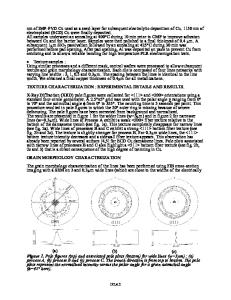
ABSTRACT The line width dependence of stress in damascene Cu was examined experimentally as well as with a numerical simulation. The measured hydrostatic stress was found to increase with increasing line width. The larger stress in an interconnect with large dimension is attributed to the larger grain size, which induce higher growth stress in addition to thermomechanical stress. A stress model based on microstructure was constructed and the contribution of the growth and thermal stress of the damascene lines were quantified using finite element analysis. It was found that the stress of the via is lower than that of wide lines when both the growth stress and thermal stress were considered. This stress gradient between via and line, which is the driving force of vacancy diffusion, is larger when the low-k with lower stiffness and higher thermal expansion is used for dielectric layer. For this reason, the Cu/low-k can be more vulnerable to stress-induced voiding. Key words: Damascene Cu, microstructure, stress, low-k dielectric, finite element analysis, xray diffraction INTRODUCTION Since the RC delay and crosstalk of the interconnects are anticipated to be the limiting factors in high performance integrated circuits, copper and low-k dielectrics are now used in place of aluminum and silicon oxide. In contrast to Al interconnects, whose reliability limitations have been well characterized through 30 years of experience, Cu interconnect reliability is still a relatively new technology. Recent progress has shown that stress voiding in Cu interconnects is now considered an important reliability concern [1-2]. Stress in the interconnects can be divided into two classes according to its origin: thermal stress, which is generated by thermal expansion mismatch between metal lines and surrounding materials, and growth stress, which is induced by the grain growth of metal lines. Grain growth is a process of grain boundary elimination. Therefore, it can cause considerable volume
B7.6.2/O11.6.2
shrinkage of the metal lines. Volume shrinkage of the metal lines with confinement by the surrounding materials causes tensile stress. For the conventional Al interconnects process, lines are formed by an etching process from continuous thin films. Generally, grain growth is completed during film deposition and annealing prior to passivation, thus the growth stress of the lines is insignificant. As a result, the major stress component is thermal stress only. On the other hand, considerable growth stress as well as thermal stress can develop in the Cu interconnects [3]. The initial grain size of the electroplated Cu is as small as few tens of nanometers. During subsequent high temperature annealing and passivation layer deposition, grain growth occurs under confinement by
Data Loading...