Lateral Solid Phase Crystallization of Amorphous Silicon Under High Pressure
- PDF / 1,503,330 Bytes
- 5 Pages / 384.12 x 617.58 pts Page_size
- 33 Downloads / 351 Views
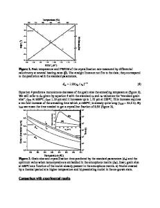
emperatures can minimize the nucleation from the a-Si/Si0 2 interface and impurity profiles in the a-Si films are not redistributed [10]. Many of the electrical properties of polycrystalline silicon depend on its grain size and defect density (e.g. microtwins in (111) orientation). However, major drawbacks of thermal annealing are the long processing time, high defect density and small grain size. It is reported that solid phase epitaxy growth rate strongly depends on the intrinsic residual strain in the amorphous silicon thin films induced by hydrostatic pressure and doping [11 ]. Ishiwara et al. [2] have reported non-hydrostatic ultra high pressure (> 1GPa) effect to grow the lateral solid phase epitaxy using amorphous silicon films deposited on Si0 2/Si structure with seeding area. The method we have described in this letter is based on the use of top polished diamond seed which is pressed onto the amorphous silicon thin films using high pressure (10-25MPa) at low processing temperatures (_25MPa), and selective nucleation of (110) grains can be achieved by surface-seeded crystallization technique. The annealing temperature has been found to play an important role in nucleation of(1 11) grains, as very fine (11l) grains (