Nucleation and Growth of Quasicrystalline Silicon Thin Films on Glass Substrate Synthesized by Ceramics Hot Wire Chemica
- PDF / 317,622 Bytes
- 6 Pages / 612 x 792 pts (letter) Page_size
- 31 Downloads / 244 Views
0910-A08-09
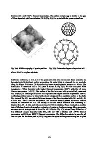
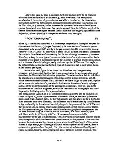
Nucleation and Growth of Quasicrystalline Silicon Thin Films on Glass Substrate Synthesized by Ceramics Hot Wire Chemical Vapor Deposition Abdul Rafik Middya1, Jian-Jun Liang1, and Kartik Ghosh2 1 Department of Physics, Syracuse University, 201 Physics Building, Syracuse, New York, 13244-1130 2 Physics, Astronomy and Materials Science, Missouri State University, 901 S. National Avenue, Springfield, Missouri, 65804 ABSTRACT In this work, we report on nucleation and growth of polycrystalline silicon thin-film on glass substrate synthesized by ceramics hot wire chemical vapor deposition. We observed perfect geometrical patterns at the surface topography of these films, i.e. “five-fold” symmetry and “sixfold” symmetry. We found “confinement of heat and photon” is a new technique in developing silicon thin-film with novel structure, i.e. quasicrystalline silicon thin-film on glass substrate. The influence of photons emitted from the hot filament on fast nucleation of nanocrystal silicon on glass substrate has been discussed.
INTRODUCTION The new thin-film growth technology, hot wire chemical vapor deposition (hot-wire CVD) has been drawing increasing attention because of the fact that we have been observing distinctly different properties, particularly structural and light-induced metastability in hot-wire CVD deposited amorphous silicon (a-Si:H) [1], nanocrystalline silicon (nano-Si) [2] and polycrystalline silicon (poly-Si) [3] thin-film. Compared to the conventional plasma-enhanced chemical vapor deposition (PECVD), hot-wire CVD deposited films exhibit comparable electronic properties, however the growth rate of hot-wire CVD films is higher by ten times compared to that of PECVD films. The major difference between the growth chemistry of hotwire CVD and PECVD process are as follows: i) absence of ionic species in hot-wire CVD process, ii) silane or germane process gases are completely decomposed by catalytic decomposition in heated filament, consequently H/(SiH)n flux arriving at the substrate surface is much higher in case of hot-wire CVD compared to that of PECVD process, iii) Si atoms directly contribute to solid silicon thin-film in hot-wire CVD as oppose to hydride radicals (SiHn) incorporate into the solid films through chemical reaction in PECVD process. There are indication that photons, particularly UV photons emitted from the heated filament influence the nucleation of silicon nanocrystal with high growth rate on glass and other foreign substrates [4]. These results raise interest on physics and chemistry of nucleation and growth of hot-wire CVD deposited nanocrystalline and polycrystalline silicon thin-film, broadly defined “thin silicon films” on glass and other foreign substrate. In this work, we attempted to isolate critical factors governing the fast nucleation Si atoms on glass substrates in hot-wire CVD thin-film growth technology.
EXPERIMENTAL DETAILS In this work, we developed silicon thin films on glass substrate with “five-fold” symmetry or “quasicrystalline”. This “new form” silic
Data Loading...