Performance of Pt-based Low Schottky Barrier Silicide Contacts on Weakly Doped Silicon
- PDF / 140,284 Bytes
- 6 Pages / 612 x 792 pts (letter) Page_size
- 47 Downloads / 381 Views
D7.9.1
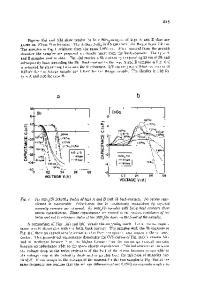
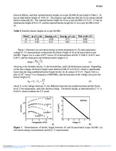
Performance of Pt-based low Schottky barrier silicide contacts on weakly doped silicon Guilhem Larrieu, Emmanuel Dubois, Xavier Wallart. Institut d’Electronique de Microélectronique et de Nanotechnologie Avenue Poincare, BP 69, 59652 Villeneuve d’Acsq, France. ABSTRACT One of the grand challenge imposed by CMOS down-scaling is the optimisation of the source/drain (S/D) architecture, e.g., dopant activation above solid solubility, steep dopant profiling, low silicide specific contact resistivity. Recently, the concept of very low Schottky barrier S/D MOSFET has emerged as a possible alternative to conventional architecture using highly doped S/D and midgap silicide ohmic contacts. For p-MOSFETs integration, platinum silicide is an excellent candidate because of its very low barrier to holes. This enables the use of a weakly doped substrate that inherently solves the aforementioned challenges due to highly doped S/D. This paper proposes a detailed study of the platinum silicidation reaction obtained by rapid thermal annealing. The analysis is based on X-ray photoemission spectroscopy (XPS), transmission electron miscrocopy (TEM) and low temperature-dependent current-voltage measurements. Using XPS analysis, it is shown that: i) an initial silicide layer is formed at room temperature, ii) three stable phases Pt, Pt2Si, PtSi can not coexist providing that iii) the annealing ambience is strictly controlled to avoid the formation of a SiO2 barrier due to oxygen penetration into the platinum overlayer. Starting from an initial 15 nm thick Pt layer subsequently annealing at 300oC, TEM cross-sections reveal that homogeneous 32 nm PtSi layers with a uniform grain size distribution are formed. Finally, current-voltage characteristics have been measured on a special test structure that accounts for the lateral disposition of S/D regions in a typical MOSFET architecture. It consists in two back-to-back Schottky contacts separated by a narrow silicon gap both on bulk silicon and Silicon-On-Insulator (SOI) substrates. Based on temperature-dependent electrical measurements (Arrhenius plot), it is shown that field emission is involved in the current transport mechanism, in addition to thermionic emission. An excellent current drive performance of 220 µA per micron width has been obtained for a 45 nm silicon gap on a 10 nm thick SOI substrate. INTRODUCTION Metal silicides are widely used in silicon based semiconductor technology and play an increasing important role in silicon integrated circuit technology as MOSFETs are shrunk below 0.1 µm of gate length. Indeed, they are very stable mechanically and against oxidation and demonstrate a low sheet resistance very close to metal. The scaling CMOS technologies [1] imposes very low S/D contact resistances that can hardly be achieved with classical architecture. An alternative consists in using S/D silicide contacts that exhibit an extremely low Schottky barrier height in order to obtain an acceptable specific contact resistance[2]. In that perspective, platinum silicide is very i
Data Loading...