The Future of Silicide for CMOS Contacts
- PDF / 1,555,973 Bytes
- 11 Pages / 417.6 x 639 pts Page_size
- 46 Downloads / 335 Views
silicide contacts to shallow p/n junction devices, the
silicide-induced junction
leakage and S/D resistance are a concern. We discuss below in some detail these requirements for silicide contacts for future CMOS generations, the ability of the self- aligned titanium or cobalt silicide (salicide) process to meet these challenges, salient features of alternative silicide processes, and the long term viability of silicides in ultimate-scaled CMOS. CONTACT REQUIREMENTS FOR 0.18 pm CMOS AND BELOW Forming contacts to the gate and S/D with low resistance metal is necessary to ensure fast circuit performance and large device drive current. Historically, the salicide process was developed as an easily implemented solution to contact the device, with several advantages including self-alignment, low resistivity of silicide materials, and mid-gap work function which helps afford a low contact resistance to n+ and p+ silicon. Additionally, the relatively low thermal budget of the silicide
35 Mat. Res. Soc. Symp. Proc. Vol. 564 ©1999 Materials Research Society
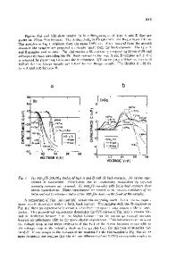
process has ensured stable p/n junctions, whose formation takes place prior to silicidation. In current CMOS, the sheet resistance (Rs) of the gate is determined by the silicide Rs (a value much lower than the underlying silicon), which is a combination of silicide thickness and resistivity. To minimize the silicide thickness required to obtain low gate Rs and ensure fast interconnect speed, it is necessary to at least maintain the current low resistivity values (about 15-20 jin-cm for C54 TiSi 2 or CoSi2 ) in future CMOS generations. The device source-to-drain resistance is determined by the combination of channel resistance, RCH, the sheet resistance in the silicon S/D (RsD), spreading resistance for the current leaving the channel and entering the S/D (Rsp), and the silicide/silicon contact resistance in the deep junction area, Rco (see Fig 1). The latter property is largely determined by the interface between the silicide and S/D, as well as the device geometry. According to a transmission line model (3) Rco (in units of Ohms) is determined by the S/D (contact) width (W) and contact length (1c, shown in Fig. 1), the silicon sheet resistance under the silicide, (-RsD), and the silicide/silicon interface resistivity, pco, (in units of f) -cm 2 ). For electrically short contacts, the contact length is sufficiently small that the current leaving the channel spreads uniformly across the contact interface, and one can use the approximation that Rco = pco(Wl) 1
(1)
For long contacts where most of the current flows from the channel into the front edge of the silicide contact,
Rco =
(pcoRsD)/ 2(W)"I
(2)
Thus, for long contacts Rco is independent of Ic. However, in scaled S/D devices, increases with Rco shorter 1c, with a transition regime around lc=0. 2 5 gm, depending
Ic silicide on the exact pco and RSD values (3). The value of pco is in turn exponentially dependent on the barrier silicide/silicon height (ýs) and the interface active doping Fig.:1. Schematic of MO
Data Loading...