Pr-O-N Dielectrics for MIS Stacks on Silicon and Silicon Carbide Surfaces
- PDF / 146,118 Bytes
- 6 Pages / 612 x 792 pts (letter) Page_size
- 58 Downloads / 328 Views
0911-B10-11
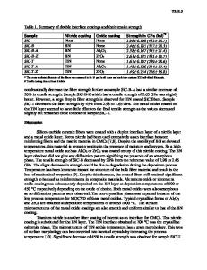
Pr-O-N Dielectrics for MIS Stacks on Silicon and Silicon Carbide Surfaces Karsten Henkel, Mohamed Torche, Rakesh Sohal, Carola Schwiertz, Patrick Hoffmann, and Dieter Schmeißer Angewandte Physik-Sensorik, BTU Cottbus, K.-Wachsmann-A. 17, Cottbus, 03046, Germany ABSTRACT We combine high-k dielectrics with wide band gap semiconductors for new possibilities for high frequency and high power applications. We investigate the dielectric properties of praseodymium based oxides by preparing MIS structures consisting of metal layer (M), PrOX (praseodymium oxide) as a high-k insulating layer (I), and silicon (Si) or silicon carbide (SiC) as semiconductor substrates (S). Our approach consists both, electrical measurements and spectroscopic characterization to analyze properties of the various interfaces within the stacks. For the electrical measurements we produce PrOX layers in the thickness range of 10nm to 240nm. We use capacitance-voltage analysis and determine permittivity values (εr) of 8 to 20 depending on physical thickness resulting in an equivalent oxide thickness (EOT) down to 5 nm. In order to prevent interface reactions and to improve the band alignment an interfacial layer is introduced into the stack between the semiconductor and the high-k material. We find aluminum oxynitride (AlON) as a suitable layer as revealed by XPS data. For AlON/PrOX stacks on Si we measured a mean interface state density of 5x10¹¹ /eVcm2 and a leakage current (1 V above flat band) below 10-5 A/cm2. INTRODUCTION Silicon carbide is a promising semiconductor material for high frequency, high power and high temperature applications [1]. Its large band gap makes it favorable for the use in high electrical fields. However, in a MIS-like structure the insulator material has to withstand even high electrical fields as the electrical field strength is scaling by Gauss's law at the interface. Therefore, the use of a high-k material may reduce the field strength in the insulator. Pr2O3 is one of the promising high-k oxides to use in microelectronic devices as an alternative dielectric of SiO2 for the next generations of microelectronic components like MIS field effect transistors [2]. We investigate the interface reactions at the metal insulator interface as well as at the insulator semiconductor interface. In our earlier experiments, reactivity of metal electrodes on thin PrOX films was addressed [3], where titanium (Ti) was found to be a suitable material for gate contacts. Therefore, in our MIS structures we use Ti on top of the oxide, followed by aluminum (Al), whereas Ti acts as a diffusion barrier against Al diffusion into the oxide. Generally, it is difficult to deposit thermally PrOX directly on the surface of the investigated semiconductors, as we found destructive interactions like graphite formation on SiC [4] and silicate formation on silicon [5]. To prevent such interface reactions suitable buffer layers should be used on the one hand. On the other hand, if we look to the tendency of decreasing of the band gap with incre
Data Loading...