32nm Node Highly Reliable Cu/Low-k Integration Technology with CuMn Alloy Seed
- PDF / 302,988 Bytes
- 6 Pages / 432 x 648 pts Page_size
- 39 Downloads / 235 Views
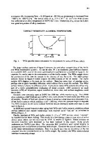
32nm Node Highly Reliable Cu/Low-k Integration Technology with CuMn Alloy Seed Shaoning Yao1, Vincent McGahay1, Matthew S. Angyal1, Andrew H. Simon1, Tom C. Lee2,Cathryn Christiansen2, Baozhen Li2, Fen Chen2, Paul S. McLaughlin1, Oluwafemi O. Ogunsola1 , Stephan Grunow1 1. IBM Microelectronics, Hopewell Junction, NY 12533 2. IBM Microelectronics, Essex Junction, VT 05452 ABSTRACT This paper introduces a highly reliable Cu interconnect technology at the 32 nm node with CuMn alloy seed. A CuMn alloy liner seed process combined with a non-gouging liner has been integrated into the minimum-pitch wiring level. Stress migration fails with CuMn seed at platebelow-via structures were shut down by a non-gouging liner process. Integration with gouging liner and non-gouging liner is compared, and results of interaction with CuMn seed are discussed in this paper. KEY WORDS Mn, Cu, electromigration INTRODUCTION It becomes challenging to achieve high reliability performance in interconnects as wire dimensions are scaled down to the 32nm node, especially for electromigration (EM) performance. EM can be thought of as the effect of an electron wind which carries metal atoms away, leaving a void behind. When this void grows to a critical size, the resistance of the metal line increases to a point where the circuit will fail. The EM failure time (t50) for pure Cu interconnects decreases dramatically as technology node goes down due to the integration challenges of ensuring good liner and seed coverage necessary for completely filling the lines with Cu coupled with the smaller wire dimension leading to a smaller void needed for failure[1]. A self-formed Mn metal cap layer has been demonstrated to improve EM performance at least by 10 times in failure time compared to pure Cu seed [1-2]. CuMn seed has been adopted in industry. Mn is very sensitive and reactive to O. Mn atoms will diffuse from CuMn alloy seed to the places where O exists and react with O forming MnO compound. This reaction is so called Mn segregation. The desirable segregation is where Mn segregates at the Cu-cap interface and self-forms a MnO cap layer. Preventing undesirable Mn segregation before Mn self-capping is a key to Back End of Line (BEOL) integration with CuMn seed. As Nogami [2] pointed out a robust non-oxidized liner is needed to isolate Mn from O-rich area: Intral Level Dielectrics (ILD). A conventional gouging liner process forming enhanced via-line contact is commonly used in Cu/ low-k (k>=3.0) integration to achieve good wiring reliability [3-6]. A similar gouging liner process was adopted at the early development phase of the 32nm node. However, it was found that a voiding issue occurred during Stress Migration (SM) at plate-below-via (PBV) structures when this gouging liner was integrated with CuMn alloy seed. This paper introduces an advanced integration technology with an alternative liner process combined with CuMn seed to resolve this stress voiding issue and achieve enhanced reliability performance.
81
EXPERIMENT Wafers were built with a single
Data Loading...