A Proposal of a Parallel Resistance Model for the Conduction Mechanism of Binary Transition Metal Oxide ReRAM
- PDF / 222,978 Bytes
- 7 Pages / 612 x 792 pts (letter) Page_size
- 48 Downloads / 262 Views
0997-I07-09
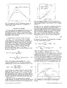
A Proposal of a Parallel Resistance Model for the Conduction Mechanism of Binary Transition Metal Oxide ReRAM Kentaro Kinoshita, Hideyuki Noshiro, Chikako Yoshida, Yoshihiro Sato, Masaki Aoki, and Yoshihiro Sugiyama Embedded Memories Development Dept., Fujitsu Laboratories Ltd., 10-1 MorinosatoWakamiya, Atsugi, 243-0197, Japan ABSTRACT A parallel resistance model (PRM), in which the total resistance, Rtotal, is given by a parallel connection of resistance of a filament, Rfila, and that of a film excluding a filament, Rexcl, was proposed to understand DC electric properties of resistive RAM (ReRAM). Here, the relationship of 1/Rtotal = 1/Rfila + 1/Rexcl is satisfied. To prove the validity of this model, the dependence of the relationship between resistance and temperature, R(T), of Pt/NiO/Pt on an area of a top electrode, S, was investigated. It was clarified that R(T) depended on S, which is the result definitely expected by the PRM. It was also clarified that smaller S is crucial to observe intrinsic properties of a filament of ReRAM. INTRODUCTION Resistive RAM (ReRAM), which consists of binary-transition metal oxides (TMOs) such as NiO and TiO2, is a promising candidate to replace flash memory as consequences of its simple cell structure, CMOS compatibility, and multi-level application [1]. However, the mechanism of resistance change has not been clarified yet. For the earliest resolution of this problem, correct understanding of the basic physical property such as the dependence of resistance on temperature, R(T), is important. However, the R(T) shows inconsistency even among the same kind of materials. For instance, Ref. [2] reported the metallic RLRS(T) in Pt/NiO/Pt, whereas Ref. [3] reported semiconductive RLRS(T) in Pt/NiO/Pt. Here, ìmetallicî and ìsemiconductiveî mean dR/dT > 0 and dR/dT < 0 respectively, and RLRS(T) is R(T) in the low resistance state. On the other hand, the location where the resistance switching occurs is becoming clear. There a re many experimental results supporting a ìfilament modelî [1, 4-7], in which the resistance switching is considered to take place in a localized current path called ìfilamentî in a TMO layer. In this paper, the authors pointed out that the filament structure can be regarded as a parallel circuit consisting of resistance of the filament, Rfila, and resistance of the TMO film excluding the filament, Rexcl, and proposed the ìparallel resistance model (PRM)î to understand DC electric properties of ReRAM universally. The dependences of the RHRS(T) and the RLRS(T) on S were measured for Pt/NiO/Pt, since S dependent R(T) was expected by the PRM. Here, S and RHRS(T) mean an area of a top electrode (TEL) and R(T) in the high resistance state, respectively. It was clarified that the influence of Rexcl on Rtotal was not negligible compared with that of Rfila, and that making S smaller is crucial to observe intrinsic properties of the filament. EXPERIMENT
A Ni film was deposited by sputtering on a Pt bottom electrode (BEL), and then oxidized to NiO by annealin
Data Loading...