A TEM Investigation of the Effects of Tensile Stress on Thin Film Microstructure and Surface Morphology
- PDF / 4,143,836 Bytes
- 6 Pages / 414.72 x 648 pts Page_size
- 40 Downloads / 326 Views
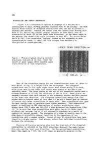
liseconds, ensuring a visually static image and full coverage of the diffraction ring during plate exposure. A 201am objective aperture (0.200 angular acceptance) was used to select the electrons to form the image. Due to the small spacing between the (Il II ring and the anomalous ring, it was impossible to form an image using only the anomalous ring, and electrons from both rings contribute to the image. The improved grain boundary contrast can be seen by comparing the bright field image in Figure 2a with the CDF image in Figure 2b. Clearly the electrons forming the anomalous ring are diffracted at the grain boundaries. While not all grain boundaries are highlighted by CDF imaging, the variation in contrast resulting from the contribution of the (111) ring allows boundaries between other grains to be detected. The CDF images were further enhanced and microstructure characterized using the image analysis program NIH Image [3]. To characterize the microstructure, grain elongation and grain size were mapped. For grain elongation mapping, NIH Image was used to fit each grain to an ellipse. Grains with major axis inclined less than 450 from the crack opening direction were then marked black. The fraction of pixels that are black therefore measures the fraction of grains elongated in the crack opening direction. Images having no grains marked black have approximately 10% black pixels from grain boundaries, so an image in which the grains are elongated in the crack opening direction will have more than 55% black pixels. For grain area mapping, a linear grey scale was used to indicate grain area with the largest grain in the image assigned a grey value of 254 (nearly black). Mean grain size is calculated as the diameter of a circle with an area equal to the mean grain area. EXPERIMENTAL RESULTS Initial Observations The deposited film initially had a mean grain size of 20nm. Following extensive annealing at 150"C (after removal from the substrate), the film had columnar grains with (I 11) fiber texture. Two different (11) ) textures developed as a result of the film's "memory" of the substrate [4]. Most of the film had grains with a narrow angular deviation from perfect (111) orientation (-1.55), but film deposited on rough regions of the substrate (such as on cleavage steps) developed orientations with larger deviation from the (111) pole (-50). Short 10-15 minute anneals at 4000 C caused the grain size to increase to 58 nm and cracks to form and propagate diffusively. Most of the cracks initiated in the 5' texture regions (i.e. most
a.
320 nm
b.
560 nm
Figure 1. Grains in front of propagating cracks are enlarged and elongated in the crack opening direction. In a, the electron beam is attenuated by a local thickness increase in the grains in front of the crack. In b, two crack tips are present and grains between them are significantly enlarged.
76
of the cracks formed in the minority component of the microstructure), but cracks were also observed to initiate in the 1.50 texture material. The origin of the cracks a
Data Loading...