Chemical, Electrical, and Structural Properties of Au/Pd Contacts on Chemical Vapor Cleaned p-type GaN Surfaces
- PDF / 927,016 Bytes
- 6 Pages / 612 x 792 pts (letter) Page_size
- 18 Downloads / 299 Views
Chemical, Electrical, and Structural Properties of Au/Pd Contacts on Chemical Vapor Cleaned p-type GaN Surfaces P. J. Hartlieb1, A. Roskowski1,B. J. Rodriguez2, R. J. Nemanich2, and R. F. Davis1 Department of Materials Science and Engineering, North Carolina State University, Raleigh, North Carolina 27695-7907 2 Department of Physics, North Carolina State University, Raleigh, North Carolina 27695-8202 1
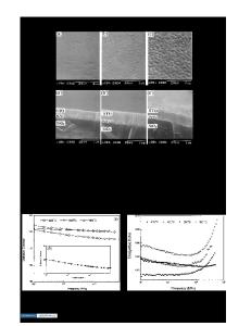
ABSTRACT The chemical, electrical, and microstructural properties of Au/Pd contacts on p-type GaN(0001) surfaces previously cleaned either ex situ or ex situ and in situ have been investigated. The in situ process involved a high temperature, NH3-based chemical vapor clean (CVC); it produced ordered, stoichiometric, p-type GaN surfaces with no detectable C and an O constituent which was subsequently reduced from 15 at% on the ex situ treated surface to 2 ± 1 at% following the CVC process. The Pd contacting layer grew epitaxially in a layer-by-layer mode on the CVC surface and formed an abrupt, unreacted metal-semiconductor interface. The Au capping layer also grew epitaxially on the Pd. Au/Pd contacts on both HCl and CVC treated surfaces exhibited identical surface roughness values (RMS) in the as-deposited state and following a 500°C anneal. Contact structures on CVC treated surfaces demonstrated excellent high-temperature microstructural stability as evidenced by the absence of significant change in the surface roughness (RMS) with successive annealing at 600 and 700°C. Identical contact structures on ex situ cleaned surfaces exhibited poor high temperature microstructural stability, as indicated by a significant increase in the surface roughness (RMS) following successive anneals at 600 and 700°C. There was a significant degradation in the morphology of both surfaces following the 800°C anneal as evidenced by the formation of large voids in the contact metallization and the exposure of the underlying p-type GaN substrate. The lowest resistance contact structures with uniform metal coverage were obtained for Au/Pd contacts on a CVC treated surface annealed at 700°C. INTRODUCTION The achievement of p-type conducting GaN has led to the development of blue and green light emitting diodes (LEDs), as well as nitride based heterojunction bipolar transistors and field effect devices [1-3]. The future improvement of these devices rests in part on a detailed understanding of the metal/p-GaN interface and the development of approaches to reduce the specific contact resistivity, which has been consistently reported between 1 x 10⁻⁴ and 5 x 10⁻¹ (Ω•cm2) [4-6]. The large work function of p-GaN (~ 6.5 eV) and the absence of any metal with a work function greater than 5.8 eV, make it impossible to select a contact metal based on matching the work functions of the materials. Additionally, there is a tenacious layer of native contamination on the as-grown surface, that is ~ 2 nm thick and adds an additional 0.2 eV to the barrier height [7,8]. The results of several studies have demonstrated a lowered specific contact resistivity f
Data Loading...