Correlation of In and Ex Situ Stress to Microstructures during Al-Induced Crystallization of PECVD Amorphous Silicon
- PDF / 486,526 Bytes
- 6 Pages / 612 x 792 pts (letter) Page_size
- 29 Downloads / 299 Views
A6.1.1
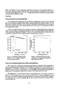
Correlation of In and Ex Situ Stress to Microstructures during Al-Induced Crystallization of PECVD Amorphous Silicon S. Ray, Y.G. Lian*, V. Sriram, D. J. Tucker and G. Z. Pan Microfabrication Laboratory, University of California at Los Angeles, Los Angeles, CA 90095 ABSTRACT We studied the correlation of in and ex situ stress to microstructures during Al-induced crystallization for structures of Al on top (AOT) and Al on bottom (AOB) of amorphous Si (a-Si) on 3000 Å SiO2 coated on Si wafers and found that a-Si deposited on PECVD SiO2 and Al increases the stress compressively, and Al deposited on PECVD SiO2 and on a-Si decreases the stress tensilely. In addition, the stress of AOB structures is in general less than that of AOT structures. Correlation of stress to microstructures indicated that the difference in microstructures between AOT and AOB results from the nature of the layer structures themselves. By using modified Stoney’s equation, the lower stress of AOB structures than AOT could be explained with existence of oxide between a-Si and Al for both AOT and AOB structures. INTRODUCTION Formation of high quality polycrystalline silicon (c-Si) at temperatures below 500 °C is vital for low temperature large area microelectronics. It was reported [1] that good quality crystalline silicon (c-Si) could be achieved through Al-induced crystallization (AIC) of amorphous silicon (a-Si) formed by plasma enhanced chemical vapor deposition (PECVD). The AIC process results in layer exchange between Al and Si through Si diffusing into crystalline Al and then precipitating within Al in the form of c-Si [1-2]. The AIC temperature was found to be as low as 200 °C for Al on top (AOT) of a-Si and 375 °C for Al on bottom (AOB) of a-Si. It is known that the quality of AIC films significantly depends on the layer structures, the stress and microstructures during AIC process. In this work we studied the correlation of in and ex situ stress to microstructures during the AIC process for both AOT and AOB structures of various aSi and Al thickness on Si wafers coated with 3000 Å PEVCD oxide. EXPERIMENTAL DETAILS The layer structures of both AOT and AOB were listed in table I. We started with initial curvature measurements of 4 inch Si wafers, followed by a layer of 3000 Å PEVCD SiO2 before the actual AOT and AOB deposition. The Al for both AOT and AOB was deposited by E-beam evaporation in a CHA Mark 40 evaporator at a rate of 2 Å/s in a vacuum of 6 x 10⁻⁷ Torr prior to deposition, and the a-Si was deposited by PECVD in a PlasmaTherm 790 system at 100 °C with a power of 300 W in He-diluted SiH4 under a pressure of 500 mTorr. To prevent the first layer of a-Si for AOT or Al for AOB from oxidation, deposition of the second layer of Al for AOT or a*
Currently with the Micro & Nanotechnology Lab at UIUC
A6.1.2
Si for AOB was immediately carried out. Following with deposition of each individual layers including the barrier PECVD oxide, wafer curvature was measured and the stress was calculated by using the total film thickness on t
Data Loading...