Damageless Magnetron Sputtering Deposition of SnO 2 :Sb Thin Films with Compensation Methods
- PDF / 344,448 Bytes
- 6 Pages / 414.72 x 648 pts Page_size
- 63 Downloads / 340 Views
Table I . Sputtering conditions for the film fabrication. ) SnO2 ( 5% Sb 20s99.99%)
Halogen
Lime Glass mmL ) (Soda 52 mm WX76
Heater Masking
100ram 0 X5mmt,
Target Substrate(Sub.)
Substrate holder
Lamp
o
0
Sheld S0Glass
--
Sub. Temperature
100
Target-Sub. Distance
40 40
RF Power
50
Sputtering Gas Pressure
5Xl0Torr
Deposition Time Presputtering Time
30 min
Shutter
40012Glass Rop hng
gas
HV Insulator
Processing
60 W
-
3
prsi
- 2.5X 10⁻²
Magnet ter
Upper 10 rmin
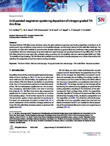
Fig. 1. Shematic diagram for RF magnetron sputtering apparatus.
Sanwa Co., R6431A; Advantest Co.) and a four probe electrode(Kullicke & Soffa Co.). Cystal structure of the films was examined on an X-ray diffraction-meter specialized for thin films(Rotaflex, Rigaku Co.). RESULTS Figure 2 shows three typical surface profiles as a function of their degree of damage. Generally, the degree of damage showed a ring pattern thus the film surface could be classified into three zone such as center, middle, and outer side. The film surface(middle zone) facing to the eroded part of the target normally showed a more serious damage. Thus, in this study, the middle zone is named as erosion(part). Figure 3 shows the effects of substrate temperature and gas pressure on the film resistivity measured on the outside zone where the resistivity is usually lower than the other two parts. From Fig. 3, it can be known that the resistivity is affected by not only gas pressure but also substrate temperature. Resistivity change over the whole substrate was also observed as functions of the substrate temperature and gas pressure, whose results are shown in Fig. 4. In Fig. 4, the above three zones are presented schematically. On the films having the profiles similar to those in Fig. 2(b) and (c), the resistivity could not be measured, these cases are expressed with the terms of partially damaged and completely damaged, respectively. As shown in Fig. 4, all the resistivities in the three zones are changed by the above two factors and their relation is also modified by the factors. XRD patterns of the same films as those in Fig. 4{Ts(substrate temperature): 3001C(}
were observed and presented in Fig. 5. Figure 5 shows that the XRD pattern is also changed by the gas pressure. In Fig. 6, the effects of RF power on the film resistivity are shown, as functions of the temperature and the position. As compared with Fig. 4(c), the resistivities at the center and the erosion parts in Fig. 6 are enhanced by a RF power increase. Effects of mask on the film resistivity are shown in Fig. 7. Figure 7 shows that
the resistivity values
of the films fabricated
with the masks became
measurable even at the center although they are higher than those without the masks.
424
film edge
(a) 20oo
prf= 50 W
A
Ts = 100 °C 0 2000C U 300 °C A
10-1
substrate .5 P = 1OmTorr 0-050W
(b)
10-2
/
P = 55mTorr
(c)
IN- 0W
I
10-3 0
5000
A
I
5
10
I
I
I
15
20
25
30
Gas pressure [mTorr] Fig. 3. Effects of substrate temperature and gas pressure on the film resistiv
Data Loading...