Effects of strain on the resonant Raman profile of metallic
- PDF / 196,402 Bytes
- 6 Pages / 595 x 842 pts (A4) Page_size
- 25 Downloads / 350 Views
0901-Rb24-04.1
Effects of strain on the resonant Raman profile of metallic carbon nanotubes A. G. Souza Filho,a N. Kobayashi,b J. Jiang,b R. Saito,b S. B. Cronin,c J. Mendes Filho,a Ge. G. Samsonidze,d G. Dresselhaus,e M. S. Dresselhausd,f a
Departamento de F´ısica, Universidade Federal do Cear´a, Fortaleza-CE, 60455-760, Brazil b Department of Physics, Tohoku University, and CREST, JST, Sendai 980-8578, Japan c Department of Electrical Engineering, University of Southern California, Los Angeles, California 90089, USA d Department of Electrical Engineering and Computer Science, e Francis Bitter Magnet Laboratory, f Department of Physics, Massachusetts Institute of Technology, Cambridge, MA 02139-4307
ABSTRACT In this paper we report the effects of strain on the electronic properties of single wall carbon nanotubes and its consequence on the resonant Raman cross section. A quantum interference effect has been predicted for the radial breathing mode spectra for metallic tubes. For metallic tubes, the lower and upper components of Eii resulting from the trigonal warping effect are affected differently and for low chiral angle they cross for some strain value. Near (at) the crossing point, the resonant Raman spectra profile exhibits a maximum (minimum) value due to a quantum interference in the Raman cross section. This Raman cross section interference effect was observed in Raman experiments carried out on isolated SWNTs. The Raman experiment performed on an isolated strained metallic SWNT supports our modeling predictions. INTRODUCTION Single wall carbon nanotubes (SWNTs) present striking properties regarding their electronic structure. [1] The atomic structure of the nanotubes is defined by the integers (n, m). The electronic transitions and optical properties show n − m family patterns.[2] The optical band gap of semiconducting SWNTs are strongly affected by strain and both theoretical [3, 4] and experimental works have been reported so far.[5, 6] Under uniaxial strain, the band gap of semiconducting SWNTs show an n − m family pattern. Most of the experimental studies on strained SWNTs have been performed on semiconducting SWNTs. In the case of metallic SWNTs there are few reports. Since metallic SWNTs do not photoluminesce, techniques such as resonance Raman spectroscopy (RRS) are needed for accessing the electronic transitions of these tubes. Nowadays, RRS studies on strained single tubes is possible.[7, 8] New physical phenomena are expected for metallic tubes since each sub-band has two components due to the trigonal warping effect.[9] The separation of the peaks depending on their (n, m) values is tunable and of the order of the energy of many Raman modes. It turns out that an understanding on how the splitting of the singularities affect the Raman intensity is very important for characterizing atomic-force modified strained SWNTs or
0901-Rb24-04.2
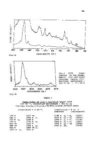
L L Figure 1: The E11 (σ)/E11 (0) ratio for different strain levels for metallic SWNTs. Data are for the lower M component of E11 .
nanotubes subjected to str
Data Loading...