First-Principles study of HfO 2 /:GaAs interface passivation by Si and Ge
- PDF / 328,865 Bytes
- 7 Pages / 612 x 792 pts (letter) Page_size
- 36 Downloads / 345 Views
1155-C09-15
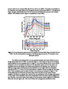
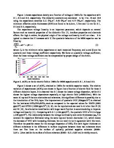
First principles study of HfO2:GaAs interface passivation by Si and Ge Weichao Wang1, Ka Xiong1, Geunsik Lee2, Min Huang2, Robert M. Wallace1,2 and Kyeongjae Cho1,2,* 1 Department of Materials Science & Engineering and 2 Department of Physics, The University of Texas at Dallas, Richardson, TX 75080 *[email protected] ABSTRACT We investigated the HfO2:GaAs interface electronic structure and interface passivation by first principles calculations. The HfO2:GaAs interface of HfO2 terminated with four O atoms and GaAs terminated two Ga atoms is found to be the most energetically favorable. It is found that the interface states mainly arise from the interfacial charge mismatch, more specifically from the electron loss of interfacial As. Si or Ge as an interfacial passivating layer helps to maintain the charge of interfacial As and hence reduce the interface states. INTRODUCTION GaAs has been of great interest in high performance channel metal-oxide-semiconductor field effect transistors (MOSFETs) because it has higher mobility and a higher breakdown field compared to Si-based devices. However, a major obstacle for integrating GaAs into MOS devices is the poor interface quality between the channel and the gate oxide. To improve the interface properties, there has been intensive research on understanding the origin of the interface states and possible ways to passivate them1-4. It is known that the GaAs native oxide1 generates a relatively high density of interfacial states inducing Fermi level pinning5. Besides native oxides, extrinsic oxides such as SiO22 may also contribute to SiO/GaAs interface states due to the partially filled dangling Si bonds. Currently, device scaling requires a high dielectric constant (k) gate dielectric oxide to replace conventional SiO2. HfO2 is one of the alternatives thanks to its high k value, superior thermal stability, and low bulk trap density. However, growing HfO2 directly on GaAs is not expected to form a high quality interface due to the formation of GaAs native oxides at the interface. To eliminate the native oxide, Ok et.al3,4 recently reported the passivation of the GaAs:HfO2 interface by Si and Ge. SiOx and GeO-like compounds were formed to avoid the native oxide aggregation, thus significantly improving the equivalent oxide thickness and leakage current of the GaAs:HfO2 interface. Nevertheless, a precise atomic scale analysis of the origin of the interface states and the passivation mechanism is still missing as compared to the HfO2:Si interface6. In this paper, we focus on the origin of intrinsic interface states and discuss the interface passivation mechanism of GaAs:HfO2 interface by Si and Ge from a theoretical point of view. COMPUTATAIONAL METHODS Our calculations are based on the density functional theory (DFT) method with the PW91 version of the generalized gradient approximation (GGA), as implemented in a plane-wave basis code VASP7-9. The pseudopotential is described by projector-augmented-wave (PAW) method1011 . An energy cutoff of 400 eV and a 8×8×1 k-poi
Data Loading...