Formation of Shallow Boron P + Junctions Using Sb Amorphization
- PDF / 778,457 Bytes
- 6 Pages / 420.48 x 639 pts Page_size
- 28 Downloads / 345 Views
FORMATION OF SHALLOW BORON P÷ JUNCTIONS USING Sb AMORPHIZATION E. Ganin, B. Davari, D. Harame, G. Scilla, and G.A. Sai-Halasz IBM T.J. Watson Research Center Yorktown Heights, NY 10598 Abstract Shallow P+ junctions have been fabricated using reverse-type dopant preamorphization by Sb. The junctions -100 nm in depth have leakage current below 10 nA/cm 2, sheet resistance less than 200 2/1" and ideality factor in the range 1.01-1.03. This type of amorphization scheme provides electrical activation of B at low temperature, which is very promising for low temperature processing applications. The importance of process optimization was demonstrated. The electrical results were correlated with residual defect structure observed by cross-sectional TEM.
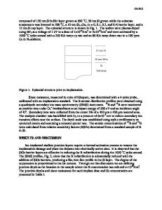
Introduction Recent studies showed that there are numerous advantages in using preamorphization by heavy ion implantation in order to fabricate shallow boron junctions1 . One of the advantages is in creating sharp crystalline / amorphous (C/A) interface with relatively low dose implant. The residual defects formed after the annealing consist mainly of end-of-range dislocation loops, which can be completely eliminated with reduced thermal budget anneal as compared to self-implantation with Si. This has been demonstrated previously' by comparing the effect of In amorphization and selfamorphization by Si on residual defect morphology and annealing kinetics. Low dose indium implantation at 40 keV was successful in forming low reverse bias leakage diodes with reasonably good sheet resistance 2 . However, the indium channeling "tails" were observed in some cases, limiting the minimum achievable junction depth to about 120 nm. The inability to avoid channeling even at a low dose ion implantation can be turned into advantage by using preamorphizing species of an opposite conductivity type than the intended dopant. In this case the implant tail instead of smearing the junction would sharpen it up, leading to a shallow well defined profile. We realized the described scheme using antimony (Sb) as the preamorphizing agent. Experimental Diodes were fabricated in N-type (100) substrates by patterning an oxide, ion implanting Sb for amorphization with energies and doses ranging from 40 keV to 60 keV at 5 2x 10l /cm 2 to 3 x 10¹⁴ /cm 2 respectively, ion implanting B at 5 keV with 1 x 101i /cm dose, annealing and metallizing using lift-off. Different rapid thermal annealing ( RTA ) and furnace annealing schedules were applied with or without low temperature regrowth ( LTR ) at 580 or 6000 C for 30 min. As a control experiment, one wafer was processed using Si self-amorphization with 30 keV Si implant at 1 x 10'5 /cm 2 dose. This wafer was annealed at 900'C for 15 min to ensure formation of a good quality junction. Sheet resistance, forward bias ideality and reverse bias leakage current measurements were performed. Leakage current measurements were made for the large 2 number (over 100) of diodes ranging from 75 /Am to 1 x 10⁶ tm 2 size. The Sb and B concentration versus depth profiles were
Data Loading...