High-Frequency Capacitance-Voltage Characteristics of Pecvd-Grown SiO 2 Mis Structure on GaN and GaN/AL 0.4 Ga 0.6 N/GaN
- PDF / 625,128 Bytes
- 4 Pages / 612 x 792 pts (letter) Page_size
- 104 Downloads / 241 Views
HIGH-FREQUENCY CAPACITANCE-VOLTAGE CHARACTERISTICS OF PECVD-GROWN SiO2 MIS STRUCTURE ON GaN AND GaN/AL0.4Ga0.6N/GaN HETEROSTRUCTURE P.Chen, Y.G.Zhou, H.M.Bu, W.P.Li, Z.Z.Chen, B.Shen, R.Zhang, and Y.D.Zheng Department of Physics, Nanjing University, Nanjing 210093, P.R.China E-mail: [email protected]
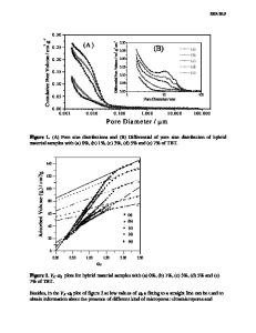
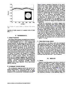
ABSTRACT Metal-insulator-semiconductor structures are fabricated by depositing SiO2 films on an MOCVD-grown n-type GaN epitaxial layer and a GaN/Al0.4Ga0.6N/GaN double heterojunction. The SiO2 films are grown by plasma-enhanced chemical vapor deposition. High-frequency C-V characteristics show the agreement of the measured C-V curve of SiO2/n-GaN with an ideal curve in deep depletion and the very small hysteresis, which indicates that the interface traps concentration in the sample is low. However, for SiO2/GaN/Al0.4Ga0.6N/GaN, the measured C-V curves show a notable flat-band shift of about 9.2 V and a typical polarization hysteresis window. These show the influence of the polarization charges in this structure. The capacitance on SiO2/GaN/Al0.4Ga0.6N/GaN reaches a minimum value under around –5V bias. The saturation at a minimum value of the C-V curve indicates the presence of holes accumulation in the MIS structure. These results imply that the piezoelectric effect in GaN/Al0.4Ga0.6N/GaN play an important role for the formation of the p-channel.
I.
INTRODUCTION
Excellent physical properties of GaN have attracted much attention for electronic device development. Up to now, a number of GaN-based field-effect transistors (FETs) have been reported[1,2]. For many applications, metal-insulator-semiconductor (MIS) technology is desirable since it would provide high DC input impedance, large gate voltage swings, normally-off operation with high source-drain blocking voltage, and high temperature operation as a result of reduced gate leakage. We have demonstrated an enhancement mode GaN-based MISHFET on a GaN/AlGaN/GaN double heterojunction with SiO2 as gate insulator[3]. Khan has also reported two MISHFETs based on AlGaN/GaN heterostructures grown on sapphire and SiC substrates respectively[12,13]. However, there is a little known about the properties of such MIS structures now. Some GaN MIS structures have been have been reported[4-6], such as SiO2/n-GaN, Si3N4/n-GaN and other oxide on n-GaN MIS structures. Arulkumaran et al.[6] compared plasma-enhanced chemical vapor deposition (PECVD) grown SiO2/n-GaN, Si3N4/n-GaN and electron beam (EB) grown SiO2/n-GaN MIS structures, and the PECVD grown SiO2/n-GaN showed the minimum interface state density (2.5×10¹¹ eV-1cm-2), together with the smallest hysteresis (0.14 V). Due to a very long response time of minority carriers in SiO2/n-GaN MIS structures and the wide bandgap of GaN, the measurements under normal conditions can only give a deep depletion capacitance-voltage (C-V) curve. It is well known that the piezoelectric effect in AlGaN/GaN heterostructure have attracted much more attention[7,8]. This effect is of obvious importance for the study of nitride-based piezodevi
Data Loading...