InGaN Double-Heterostructures and DH-LEDs on HVPE GaN-on-Sapphire Substrates
- PDF / 309,668 Bytes
- 6 Pages / 414.72 x 648 pts Page_size
- 7 Downloads / 346 Views
INTRODUCTION Conventional growth of III-nitrides on sapphire requires the use of a lowtemperature buffer layer to promote nucleation and achieve single crystal films. Alternatively, thick GaN deposited by HVPE directly on sapphire can be used as a
template for MOVPE growth. In addition to significantly reducing the MOVPE growth complexity, HVPE GaN templates offer an improvement in the properties of subsequently deposited layers. HVPE GaN with thickness of the order of 200 gtm has been demonstrated with defect densities as low as 5x 106 cm-2 .1 The use of this material as a template for optoelectronic devices may have a significant impact on their lifetimes and performance. Thinner HVPE GaN base layers, with thickness on the order of 10 lim, are currently produced over 2" sapphire substrates. These GaN-on-sapphire substrates have high crystalline quality, offer a homoepitaxial template for GaN growth, and provide enhanced lateral conduction for optoelectronic device fabrication on sapphire. In this paper we present growth results of InGaN/GaN double-heterostructures (DH) and DHLEDs on HVPE GaN-on-sapphire substrates, with crystalline and optical properties comparable to the best reported in the literature. EXPERIMENT MOVPE growth on GaN-on-sapphire substrates was initiated by bringing the substrate directly to the GaN growth temperature under an ammonia flux, eliminating the need for complicated buffer layer growth. Details on our experimental setup, as well as on 1047 Mat. Res. Soc. Symp. Proc. Vol. 482 0 1998 Materials Research Society
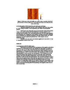
2 typical GaN growth conditions are reported elsewhere. GaN films deposited on the HVPE substrates were very smooth and specular, and showed improved structural and optical properties compared to the starting substrate. Table I presents typical results obtained from MOVPE GaN films deposited on HVPE GaN substrates, and the relative properties of the starting substrates.
Table 1. Typical properties of MOVPE GaN films deposited on HVPE GaN substrates MOVPE GaN HVPE GaN 4 gtm 8 2 12 rm 2 Thickness 8x 10 cm Ix 109 cm2 Defect density 190 arcsec arcsec 280 XRD FWHM 3
5
Carrier Conc.
I x I018 cm- (n-type)
High resistivity (> I x 10 f".cm)
PL FWHM (Band-edge) AFM RMS roughness
45 meV 77 nm (80x80 gtm 2 area)
32 meV 14 nm (80x80 gtm 2 area)
In order to grow InGaN films on the HVPE GaN-on-sapphire substrates, an initial 0.5 jgm GaN layer was first deposited on the 12 jgm HVPE base-layer. This initial layer provided a smooth starting surface for InGaN nucleation, as well as forming the bottom confining layer of the heterostructure. Typical growth temperatures used to obtain high quality In, Gal, N (0
Data Loading...