Interplay Between Copper Electroplating and Chemical Mechanical Planarization
- PDF / 155,928 Bytes
- 8 Pages / 612 x 792 pts (letter) Page_size
- 65 Downloads / 412 Views
Interplay Between Copper Electroplating and Chemical Mechanical Planarization David K. Watts1, Yusuke Chikamori, Tatsuya Kohama, Norio Kimura, Koji Mishima, and Akihisa Hongo Ebara Corporation, Fujisawa, Japan 1 Ebara Technologies, Inc., San Jose, CA, USA INTRODUCTION The introduction of Chemical Mechanical Polishing (CMP) into semiconductor device processing brought a significant need for wet chemistry research and development in this industry. With the transition from aluminum to copper for advanced interconnect metallization came a tremendous amount of electrochemical research and process development towards a production worthy copper CMP process capable of meeting the stringent specifications of dual damascene integration. In addition, the dual damascene integration scheme introduced copper deposition challenges that brought significant activity in developing another wet chemistry process, electroplating. These two sequential, chemical processes have been shown to have significant interaction that has created significant challenges in process integration. Critical issues based on the interaction between these two processes have been explored at Ebara. Such issues include global uniformity, local morphology variation, post CMP voids or pits, or transient changes in copper structural and compositional properties. For example, a non-uniform copper clearing pattern observed during copper CMP can be compensated for in the CMP process but may be indicative of non-uniform deposition, or demonstrate the need for a post deposition anneal that gives a more uniform distribution of copper microstructure across the wafer. As another example, compositional changes to copper electroplating bath chemistry can achieve high aspect ratio, “bottom-up” trench fill, but can present local, pattern dependant, challenges for copper CMP. Such process integration issues can be categorized based on two scales, wafer level and device level. Due to the large scope of this topic, this paper (Part 1) will focus on wafer level interaction and present just some of the copper electroplating and copper CMP results that highlight the process integration challenges between these two wet processes. EXPERIMENTAL DETAILS All CMP and copper electroplating experiments were performed on 200 mm blanket and patterned copper wafers using Ebara’s integrated CMP-clean 200 mm systems, EPO222 and F*REX200, and Ebara’s standard and advanced copper electroplating systems. Blanket 200 mm copper-seeded wafers were electroplated to a final copper thickness of 1.5 um.
M3.1.1
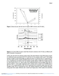
RESULTS The need for annealing after interconnect copper electroplating has been demonstrated previously. The results obtained here for the impact of anneal temperature and anneal time are shown in Figures 1 (a) and (b).
Figure 1 (a). Impact of Anneal Temperature on copper sheet Resistance at Constant Time.
Figure 1 (b). Impact of Anneal Time on copper sheet Resistance at Constant Temperature.
M3.1.2
Significant improvement was observed in copper conductivity with a postelectrodeposition a
Data Loading...