Low Temperature MOCVD Growth of V/VI Materials via a Me 3 SiNMe 2 Elimination Reaction
- PDF / 398,241 Bytes
- 6 Pages / 414.72 x 648 pts Page_size
- 34 Downloads / 258 Views
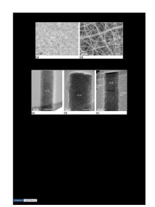
ABSTRACT Films of M2Te 3 (M = Sb, Bi) were grown on Si(lll) cut 4' off-axis and GaAs(100) substrates between 25°C and 150'C in a low pressure MOCVD reactor via a novel N,Ndimethylaminotrimethylsilane (Me 3SiNMe 2) elimination reaction using M(NMe 2)3 (M = Sb, Bi) and (Me 3Si) 2Te. X-ray diffraction data indicated that the crystallinity and crystallite orientation of the resulting films were dependent on the substrate structure and growth temperature. Amorphous films were deposited below 50'C. Films deposited at 75'C for Sb2Te 3 and 125'C for Bi 2Te 3 were highly oriented with the (015) reflection plane parallel to the substrate surface. Films of Sb2Te 3 deposited at 150'C were highly oriented with the (00t) reflection planes parallel to the substrate surface. The electrical properties and presumably the composition of Bi 2Te3 films deposited on Kapton was independent of the V/VI precursor ratio used. This unique deposition reaction provides an alternative route to prepare group V chalcogenide materials which have potential applications in solar cells, reversible optical storage, and thermoelectrics. INTRODUCTION The V/VI semiconducting compounds are the most efficient materials for thermoelectric cooling (TEC) devices found to date. For optimal thermoelectric device performance solid solution alloys are used where the best n-type material is made of Bi 2Te3 with 10 mol% Bi 2 Se 3 and the best ptype material is Bi 2Te 3 with 75 mol% Sb2 Te3 [1]. The alloy materials which are used in TEC device fabrication are commonly prepared as boules from high temperature methods which are subsequently cut to form device segments or crushed and pressed into device segments. As a result, most studies of V/VI compounds have been conducted using bulk samples and only limited attention has been directed to thin films of these materials. Bi 2Te 3 and Sb2 Te 3 films have been deposited by various techniques including molecular beam epitaxy [2], flash evaporation [3], sputtering [4], and ionized cluster beam (ICB) [5] methods. All of these methods require sophisticated UHV systems and careful control of fluxes to obtain stoichiometric films. We previously reported a novel technique to prepare these materials as powders and thin films directly from reactive organometallic precursor compounds using reaction 1 [6]. This method relies on the self limiting reaction to produce films of V/VI material of the proper stoichiometry. A more detailed account of Bi 2Te 3 and Sb2Te 3 film depositions using this method will be presented in this paper. 2M(NMe 2 )3
+
3(Me 3 Si) 2 Te
-
'
M = Sb, Bi
M2 Te 3
+
6Me 3 SiNMe 2
FILM
271 Mat. Res. Soc. Symp. Proc. Vol. 410101996 Materials Research Society
(1)
Bi 2Te 3 and isomorphous Sb2 Te3 crystallize with a rhombohedral lattice (space group R3m) however their structure is usually referred to using a hexagonal unit cell for connivance sake. The compounds have a layer-type lamellar structure with weak bonding and Van der Waals interactions between tellurium layers providing an easy cleavage plane i
Data Loading...