Low Temperature Synthesis of Nanocrystalline Silicon and Silicon Oxide Films by Plasma Chemical Vapor Deposition
- PDF / 565,630 Bytes
- 6 Pages / 612 x 792 pts (letter) Page_size
- 61 Downloads / 487 Views
1066-A06-10
Low Temperature Synthesis of Nanocrystalline Silicon and Silicon Oxide Films by Plasma Chemical Vapor Deposition Atsushi Tomyo1, Hirokazu Kaki1, Eiji Takahashi1, Tsukasa Hayashi1, Kiyoshi Ogata1, and Yukiharu Uraoka2 1 Process Research Center, R & D Laboratories, Nissin Electric Co., Ltd., 47 Umezu, Takase, Ukyo-ku, Kyoto, 615-8686, Japan 2 Graduate School of Materials Science, Nara Institute of Science and Technology, 8916-5 Takayama, Ikoma, Nara, 630-0192, Japan ABSTRACT We have investigated the control method of nanocrystalline silicon (nc-Si) structures prepared by inductively coupled plasma chemical vapor deposition (ICP-CVD). In order to determine the diameter and surface density of nc-Si dots, plan-view transmission electron microscopy (TEM) was carried out. It was showed that spatially isolated nc-Si dots were synthesized and that the diameter and the standard deviation could be well controlled with substrate temperature, gas pressure and synthesis time. In particular, the mean diameter of 3.3 ± 0.6 nm and surface density of 1 × 1012 cm-2 were achieved with the optimum condition. Using the same ICP-CVD system, we have also obtained a SiO2 film which has good electrical characteristics.
INTRODUCTION Nanocrystalline silicon (nc-Si) dot has attracted much attention because it exhibits unique features, such as Coulomb blockade, light emission and absorption [1,2]. For example, quantumdot floating gate memory devices have advantage of the high reliability with respect to the breakdown of tunnel oxide [3]. In the practical applications of nc-Si dots in quantum effect device, it is important to control the size and surface density. In case of floating gate memory devices with nc-Si dots embedded in SiO2, the diameter is theoretically expected to be less than 10 nm for room-temperature operation and the surface density should be as high as 1012 cm-2 to gain a sufficient voltage shift for memory operation [4]. In addition, low temperature synthesis of nc-Si dots and SiO2 films is desirable for high throughput in mass production and use of substrates which consist of low melting point materials. The authors have already reported that nc-Si dots could be synthesized at the initial stage of microcrystalline silicon (µc-Si) films, with which a bottom-gate thin-film transistor exhibited a field-effect mobility of 3 cm2/(V·sec) [5]. The deposition of µc-Si films was performed by ICPCVD with low inductance antenna (LIA) units which were installed inside of a vacuum container so that the induced electric field from an antenna could be used effectively. By reducing the antenna inductance and fully covering antenna conductors with insulator, the plasma potential would decrease and thus the plasma damage to the underlayer could be suppressed [6]. It is worthy to mention that this plasma source could be applicable for the large-area deposition by increasing the number of antenna units.
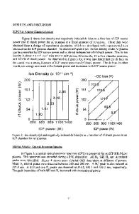
In this study, nc-Si synthesis and SiO2 deposition were also performed by ICP-CVD with LIA units, expecting that high density pla
Data Loading...