Monitoring the growth of microcrystalline silicon deposited by plasma-enhanced chemical vapor deposition using in-situ R
- PDF / 215,034 Bytes
- 5 Pages / 432 x 648 pts Page_size
- 57 Downloads / 310 Views
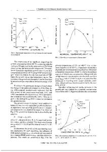
Monitoring the growth of microcrystalline silicon deposited by plasma-enhanced chemical vapor deposition using in-situ Raman spectroscopy S. Muthmann*, F. Köhler, M. Hülsbeck, M. Meier, A. Mück, R. Schmitz, W. Appenzeller, R. Carius and A. Gordijn IEK5-Photovoltaik, Forschungszentrum Jülich, D-52425 Jülich, Germany ABSTRACT A novel setup for Raman measurements under small angles of incidence during the parallel plate plasma enhanced chemical vapor deposition of μc-Si:H films is described. The possible influence of disturbances introduced by the setup on growing films is studied. The substrate heating by the probe beam is investigated and reduced as far as possible. It is shown that with optimized experimental parameters the influence of the in-situ measurements on a growing film can be neglected. With optimized settings, in-situ Raman measurements on the intrinsic layer of a microcrystalline silicon solar cell are carried out with a time resolution of about 40 s corresponding to 20 nm of deposited material during each measurement. INTRODUCTION Hydrogenated microcrystalline silicon (μc-Si:H) is a material of a great technological relevance. The applications range from thin-film transistors to large-scale devices like solarcells. It is well known that μc-Si:H is a phase mixture of amorphous and crystalline material. A well established way to deposit thin μc-Si:H films is the plasma enhanced chemical vapor deposition (PECVD). This type of deposition usually leads to an evolution of the complex structure in growth direction [1,2]. A lot of effort has been made to understand and control the growth process of μc-Si:H [3 - 6]. The methods that are available up to now have in common that they are more or less indirect ways to obtain information about material properties. We present results obtained with a new experimental setup that enables Raman measurements on thin silicon films during their deposition with PECVD in parallel plate configuration. With this technique direct information about the composition of a growing layer can be obtained during the growth. EXPERIMENT The in-situ Raman setup was included into an existing multi-chamber PECVD system for state-of-the-art thin-film silicon solar cells. Deposition of the intrinsic layers and the Raman measurements were carried out in a chamber containing a showerhead electrode. The doped layers were deposited in separate chambers to avoid cross contamination. Intrinsic layers were deposited at a pressure of 13 mbar with a heater temperature of 200 °C at an excitation frequency of 13.56 MHz which is the industrial standard for large area depositions. The power density was in the range of 0.2 W/cm². In-house produced texture etched zinc oxide covered glass with a size of 10x10 cm² was used as a substrate.
387
The source gases for the deposition were silane and hydrogen. The parameter used to describe the amount of silane in the source gas composition is the silane concentration SC: SC =
SiH 4 SiH 4 + H 2
(1)
It is well known that the amount of amorphous phase in a μc-Si:H
Data Loading...