Next Generation of Thin Film Transistors Based on Zinc Oxide
- PDF / 226,909 Bytes
- 6 Pages / 595 x 842 pts (A4) Page_size
- 10 Downloads / 445 Views
E1.9.1
Next Generation of Thin Film Transistors Based on Zinc Oxide E. Fortunato, P. Barquinha, A. Pimentel, A. Gonçalves, L. Pereira, A. Marques, R. Martins Materials Science Department/CENIMAT, Faculty of Sciences and Technology of New University of Lisbon, Campus da Caparica, 2829-516 Caparica, Portugal. ABSTRACT We report high performance ZnO thin film transistor (ZnO-TFT) fabricated by rf magnetron sputtering at room temperature with a bottom gate configuration. The ZnO-TFT operates in the enhancement mode with a threshold voltage of 19 V, a field effect mobility of 28 cm2/Vs, a gate voltage swing of 1.39 V/decade and an on/off ratio of 3×10⁵. The ZnO-TFT present an average optical transmission (including the glass substrate) of 80 % in the visible part of the spectrum. The combination of transparency, high field-effect mobility and room temperature processing makes the ZnO-TFT a very promising low cost optoelectronic device for the next generation of invisible and flexible electronics.
INTRODUCTION Transparent electronics are nowadays an emerging technology for the next generation of optoelectronic devices. Oxide semiconductors are very interesting materials because they combine simultaneously high/low conductivity with high visual transparency and have been widely used in a variety of applications (e.g. antistatic coatings, touch display panels, solar cells, flat panel displays, heaters, defrosters, optical coatings, among others) for more than a halfcentury. Transparent oxide semiconductor based transistors have recently been proposed using as active channel intrinsic zinc oxide (ZnO). These transistors present an on-to-off ratio of about 106 and relative low channel mobilities between 1 and 3 cm2/Vs [1-6]. The main advantage of using ZnO deals with the fact that it is possible to growth at/near room temperature high quality polycrystalline zinc oxide, which is a particular advantage for electronic drivers, where the response speed is of major importance. Besides that, since ZnO is a wide band gap material (3.2 eV), it is transparent in the visible region of the spectra and therefore, also less light sensitive. Besides these works Nomura et al. [7] proposed also recently a transparent transistor using as active channel a single crystal of InGaO3(ZnO)5. The most impressive aspect of this transistor is the high channel mobility of 80 cm2/Vs, mainly due to the absence of structural defects and to a low carrier concentration. In this work we report results concerning the fabrication and characterization of a high fieldeffect mobility ZnO-thin film transistor (ZnO-TFT) deposited at room temperature by rf magnetron sputtering where the gate dielectric is based on silicon oxynitride and the drain and source are based on highly conductive gallium doped zinc oxide (GZO). Moreover, the processing technology used to fabricate this device is relatively simple and it is compatible with inexpensive plastic/flexible substrate technology.
E1.9.2
EXPERIMENTAL DETAILS The ZnO films were deposited onto soda lime glass sub
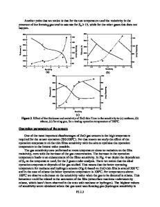
Data Loading...