Optical and electrical properties of solid photocatalyst Bi 2 InNbO 7
- PDF / 70,980 Bytes
- 3 Pages / 612 x 792 pts (letter) Page_size
- 90 Downloads / 236 Views
Jinhua Ye National Research Institute for Metals, 1-2-1 Sengen, Tsukuba, Ibaraki 305, Japan
Hironori Arakawa National Institute of Materials and Chemical Research, 1-1 Higashi, Tsukuba, Ibaraki 305, Japan (Received 13 March 2000; accepted 24 July 2000)
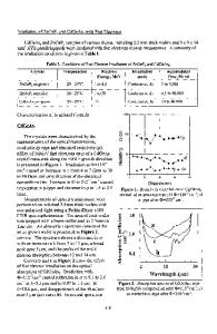
A polycrystalline sample of Bi2InNbO7 was synthesized by a solid-state reaction and characterized by powder x-ray diffraction and Rietveld structure refinement. The optical absorption and electrical properties of Bi2InNbO7 were investigated. It was found that the Bi2InNbO7 compound exhibited a direct gap semiconducting behavior. Conductivity measurement showed the compound had an activation energy of 2.62(5) eV. Ultraviolet–visible diffuse reflectance spectroscopy measurement revealed that the band gap of Bi2InNbO7 is about 2.7(4) eV.
Since the discovery of the photocatalytic splitting water on Pt/TiO2 electrodes,1 the study of photolysis of water with a semiconductor as the catalyst has attracted much interest. Later advances in materials fabrication led to the discovery that metal oxide semiconductors with tunnel or layered perovskite structures have the possibility to decompose water with higher activity.2,3 Unfortunately, the number of photocatalyst materials is limited. There is an urgent need to develop a new type of photocatalyst materials with higher activity. Very recently, we reported the characterization of a new solid photocatalyst Bi2InNbO7. The photocatalyst shows that the total volume of evolved H2 was attained with 12 mmol/g of catalyst when this reaction achieved 100 h in Pt/CH3OH/H2O solution. The value corresponded to a 9.3 mol ratio of H2 evolution to catalyst. The H2 and O2 evolutions were generated from pure H2O with ultraviolet irradiation, not using other co-catalysts. Furthermore, we found that oxygen formed is photoabsorbed at the surface of the Bi2InNbO7 particles.4 The process for photocatalysis of semiconductors is explained generally that the photon is absorbed directly by the band gap of the conventional semiconductor, generating electron–hole pairs in the conduction band and the valence band. To gain a better understanding of photocatalytic efficiency of the photocatalyst, it is important to investigate the optical and electrical properties of the photocatalyst.
a)
Address all correspondence to this author. e-mail: [email protected]
Herein, we report the synthesis and characterization of optical and electrical transport properties of the Bi2InNbO7 photocatalyst. A structure determination from Rietveld refinement of powder x-ray diffraction (XRD) data is presented. This is the first report on physical properties of the Bi2InNbO7 photocatalyst. The polycrystalline sample of Bi2InNbO7 was prepared by the solid-state reaction method using highpurity grade chemicals of In2O3, Bi2(CO3)3, and Nb2O5. In2O3 was dried at 700 °C and Nb2O5 at 600 °C before use. The stoichiometric amounts of precursors were mixed and pressed into small columns. The small columns were sintered in an alumina crucible using an electric furnace. The sintered sample
Data Loading...