Real Time Study of Cu Diffusion through a Ru Thin Film by Photoemission Electron Microscopy (PEEM)
- PDF / 751,561 Bytes
- 6 Pages / 612 x 792 pts (letter) Page_size
- 97 Downloads / 427 Views
0914-F05-07
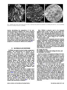
Real Time Study of Cu Diffusion through a Ru Thin Film by Photoemission Electron Microscopy (PEEM) Wei Wei1, Gang Xiong2, Y.-M. Sun1, Alan G. Joly2, Kenneth M. Beck2, J. M. White1, and Wayne P. Hess2 1 Department of Chemistry and Biochemistry, The University of Texas at Austin, Austin, TX, 78712 2 Chemical Structure and Dynamics, Pacific Northwest National Laboratory, Richland, WA, 99352 ABSTRACT We demonstrate the efficacy of Photoemission Electron Microscopy (PEEM) as a tool to detect metal diffusion processes at nanoscale spatial resolution in real time. For a sample comprising a nominally 1 nm physical vapor-deposited (PVD) Ru thin film covering a thick Cu substrate, in-situ PEEM images display the appearance of bright features on a dark background as the temperature increases. These bright features are attributed to Cu diffusion through the Ru film, which in turn results in stronger surface photoelectron emission due to the lower work function of Cu compared to Ru. INTRODUCTION Photoemission electron microscopy (PEEM) is a variant of electron microscopy that images photoelectrons generated by ultraviolet, laser or X-ray sources. Low-energy PEEM is a non-intrusive surface-sensitive technique because the attenuation length of the low-energy (∼1 eV) photoelectrons used for imaging is approximately 1 nm [1-4]. Since the emission of lowenergy photoelectrons is sensitive to the surface work function, the image contrast often reflects surface chemical composition, phase [5], crystal orientation, and surface dipole [6, 7]. In our PEEM experiments, images can be captured at video rates over a micron-scale field of view. Since imaging contrast depends upon microscopic structure and work function, different elements and the reaction kinetics of adsorbed molecules (atoms) can be imaged as a function of surface structure and temperature. The capability to take images in real time as a function of temperature is an advantage of PEEM over other scanning probe techniques [8]. Recently, in copper (Cu) interconnect technology, ruthenium (Ru) has been used as a Cu diffusion barrier, since Ru can improve adhesion of an overlayer of Cu and allow direct electroplating of Cu on the barrier without a Cu seed layer [9, 10]. The low solubility of Ru in Cu [11] is an especially favorable attribute for a barrier material. Chan [9] has reported that ~20 nm of Ru effectively prevents Cu diffusion up to 450 °C and Arunagiri [12] demonstrated that 5 nm of Ru can function as a directly platable Cu diffusion barrier up to at least 300 °C vacuum annealing. In this paper, we describe the utility of photoemission electron microscopy (PEEM) to measure real time surface changes due to Cu diffusion through a nominally 1 nm thick Ru film. These PEEM results are part of an in-depth study to be reported elsewhere that connects PEEM with atomic force microscopy (AFM), scanning electron microscopy (SEM) and X-ray photoelectron spectroscopy (XPS) of Ru-Cu interfaces. This study demonstrates that PEEM has
valuable potential for observing Cu d
Data Loading...