Segregation of aluminum in Si and SiO 2 films deposited by plasma-enhanced chemical vapor deposition in fabrication of l
- PDF / 273,631 Bytes
- 6 Pages / 612 x 792 pts (letter) Page_size
- 30 Downloads / 306 Views
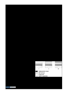
Metal contamination in Si and SiO2 films deposited by plasma-enhanced chemical vapor deposition (PECVD) in the fabrication of low-temperature poly Si thin-film transitor was investigated. Aluminum was the major metal impurity to have the highest concentration. Segregation of Al was always observed in the films deposited at temperatures above 400 °C. The impurity level in the segregated region was 1018 ∼ 1020 atoms/cm3 for Al, while the concentration in matrix was about 1016 atoms/cm3. From the transmission electron microscopy image, the Al segregated region contains small-size Al precipitates. Although the Al impurity level of 1016 atoms/cm3 did not cause any serious degradation of device performance, the level of 1018 atom/cm3 and higher can induce a fatal degradation of the threshold voltage. This study revealed that the Al originated from the PECVD chamber, carbon precipitates provided the preferred sites for Al precipitates, and the solubility and diffusivity of Al in Si accelerated the segregation of Al.
I. INTRODUCTION
In integrated circuit and solar cell fabrication, the metal impurities cause structural defects at semiconductor-insulator interface, increase leakage current of p–n junctions, reduce minority carrier lifetime, and bring early oxide breakdown.1 The impurities exist in the device being dissolved in matrix or precipitated. While recombination or generation occurs with both precipitated and dissolved impurities, electrical shorts in silicon devices are generally caused by precipitates. Electronic shortening also depends on the concentration of structural defects in the device region. Metal impurities generally precipitate heterogeneously at structural defects and the precipitates can induce device failure. The evidence for this occurring was found for both integrated circuits2 and solar cells,3 and the efforts to characterize and identify the precipitates were made.4 Also, it is reported that the main impurity metal is Fe element, and the Fe contamination in Si is attributed to the common use of stainless steel in the equipment and chemical solutions. Therefore, it was recommended that Fe impurity should be controlled below 1010 atoms/cm3 for future Si processing.1,5 The amorphous Si (a–Si) thin-film transistor (TFT) process or low-temperature poly Si (LTPS)-TFT process uses mainly plasma-enhanced chemical vapor deposition (PECVD) to make a semiconducting layer and insulator layer, while the fabrication process of integrate circuit or J. Mater. Res., Vol. 18, No. 4, Apr 2003
http://journals.cambridge.org
Downloaded: 24 Mar 2015
solar cell uses Si wafers and thermal oxides. Thus, it is inevitable that the TFT devices have a much higher level of contamination than integrated circuits or solar cell devices. This is because the PECVD process chamber is composed of Al or Al2O3 and can be a source of metal contamination. The contamination problem is expected to be more serious in the LTPS-TFT process compared with the a–Si TFT process, as the former process uses higher a–Si deposition temperature o
Data Loading...