Structural Characterization of Low-Temperature InN Buffer Layer Grown by RF-MBE
- PDF / 554,279 Bytes
- 6 Pages / 612 x 792 pts (letter) Page_size
- 66 Downloads / 300 Views
Y10.68.1
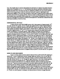
Structural Characterization of Low-Temperature InN Buffer Layer Grown by RF-MBE T. Araki and Y. Nanishi Dept. of Photonics, Ritsumeikan University 1-1-1 Noji-higashi, Kusatsu, Shiga 525-8577, Japan ABSTRACT The microstructure of an InN buffer layer grown on (0001) sapphire at low temperature by radio-frequency molecular beam epitaxy (RF-MBE) is characterized by transmission electron microscopy. The low-temperature InN buffer layer is found to contain local inhomogeneous regions of island-like grains surrounded by misoriented InN grains and inclusions of cubic phase. The generation of such anti-phase InN nuclei near the island-like grains is expected to give rise to defects at the interface. It is considered that these anti-phase InN nuclei are formed by local fluctuations of stoichiometry due to inadequate surface migration during the growth of the InN buffer layer, indicating the important of controlling the surface stoichiometry during InN growth.
INTRODUCTION InN is a promising semiconductor material for use in high-speed electronic devices based on its theoretical high peak velocity (> 1×108 cm/s) and saturation velocity (4.2×107 cm/s) compared to other III-nitride materials (GaN, AlN) [1, 2]. Furthermore, recent experimental results have demonstrated that the fundamental bandgap energy of InN is around 0.7–0.8 eV [3-7], which is much narrower than the widely accepted value of 1.9 eV [8, 9]. This discovery has presented new applications of InN-based nitride semiconductors such as in light-emitting devices over a broader wavelength range from infrared to ultraviolet, as well as high-efficiency solar cells. For a long time, however, the low dissociation temperature of InN and the extremely high equilibrium vapor pressure of nitrogen have hindered successful growth of high-quality InN films. During the past few years, the development of growth techniques, particularly the advances in molecular beam epitaxy (MBE), have resulted in significant improvements in the quality of fabricated InN films. InN films with room-temperature Hall mobility of more than 1000 cm2/Vs and carrier concentrations of the order of 1018 cm-3 have been successfully produced by several groups using MBE [10-14]. One of the key issues to obtain such high-quality InN films is the insertion of a buffer layer between the highly mismatched substrate material and the InN epitaxial layer. Similar to the low-temperature (LT) AlN buffer layer required for successful growth of high-quality GaN [15], the buffer layer plays a very important role in InN film growth. To date, various buffer layers (e.g., AlN [16, 17], LT-InN [14, 18], LT-InN/LT-GaN [12] etc.) have been used for InN growth on (0001) sapphire, and the preparation of a buffer layer has been found to be essential to obtain high-quality InN films. However, InN films of device quality have not yet been achieved, suffering from high residual carrier concentrations of the order of 1018 cm-3 and high threading dislocations densities of more than 1010 cm-2. Therefore, the role of the buffer
Data Loading...