Study on ZrO 2 Deposited Directly on Si as an Alternative Gate Dielectric Material
- PDF / 1,770,217 Bytes
- 6 Pages / 415.8 x 637.2 pts Page_size
- 73 Downloads / 286 Views
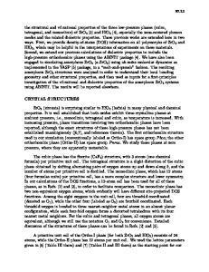
and spin-dried with N2. ZrO 2 was reactive-magnetron-sputtered from a 4-inch diameter Zr target (99.7% pure). The base vacuum of the sputtering chamber is about 2x10⁻⁷ Torr. The target-tosubstrate distance is about 30cm. The substrate can be heated by lamps mounted above the wafer, and sputtering temperature ranged from room temperature to 300'C. The pressure was 40mTorr, and the power ranged from 200W to 400W. The ZrO 2 films were deposited in the following manner. Initially, a thin layer of Zr was sputtered in an Ar ambient. Next, 2sccm of 02 was introduced to the chamber during sputtering in order to oxidize the Zr. The total pressure during the Ar + 02 sputtering remained at 40mTorr, and there was some ZrO2 deposition occurring at this time. The initially sputtered Zr layer serves as a barrier layer for oxidation. This process also prevents the target from being oxidized. Each sputtering cycle consists of one Aronly sputtering and one Ar + 02 sputtering and oxidization process. After ZrO 2 sputtering, the film was furnace annealed or rapid thermal annealed in a N 2 ambient. Pt was sputtered as the electrode. It was patterned by lithography and etched with aqua regia solution (H2 0:HCI:HNO 3 = 5:7:1) at 80'C. Al was evaporated on the backside of the wafer to ensure a low contact resistance. ZrO 2 material properties were characterized by ellipsometer, X-ray diffraction (XRD), Transmission Electron Microscopy (TEM), Rutherford Backscattering Spectroscopy (RBS), and X-ray Photoelectron Spectroscopy (XPS). Capacitance-Voltage (C-V), LeakageVoltage (I-V), and time-dependent dielectric breakdown (TDDB) were measured using HP4156 and 4194. RESULTS AND DISCUSSIONS Structural and material properties of sputtered ZrO2 thin film Fig. 1 shows the refractive index of sputtered ZrO 2 after furnace annealing for 5minutes in N 2 ambient. For films sputtered at 300W and 300'C, the refractive index is close to the ideal (2.2); while for films sputtered at 200W and room temperature, the refractive index is lower. For both films, the refractive index remains fairly stable even after 800'C annealing. Russak et al [10] reported that for 2000A thick ZrO 2, higher sputter rates resulted in higher refractive index and denser film. The sputter rate at 200W is about 17.5A/min while at 300W is about 85.OA/min. The higher sputter rate contributes to the higher refractive index. Since annealing of the film did not change the refractive index significantly, the higher refractive index likely comes from the higher sputter rate at 300W, rather than the higher sputtering temperature. 2.10..
'
2.05 x
2.0
t;
.
.
2.00
-
- 3
Sputter at 300W,300"C anneali ---- ONanel-
S 1.95k
1.900,a
1
1.850Sputter at200W,R.T.
1.75 t
. As dep 600C 700C 800C Annealing Temperature (C )
Fig. 1. The refractive index of sputtered ZrO 2 films, higher sputter rate results in higher refractive index,
Fig. 2. TEM pictures of ZrO 2/Si after 550 0 C, 5', N 2 anneal. An amorphous ZrO 2 structure can be seen with a 15A interfacial layer.
264
The crystallinit
Data Loading...