Surface Morphology of MBE-grown GaN on GaAs(001) as Function of the N/Ga-ratio
- PDF / 6,153,295 Bytes
- 11 Pages / 612 x 792 pts (letter) Page_size
- 80 Downloads / 327 Views
Internet Journal Nitride Semiconductor Research
Surface Morphology of MBE-grown GaN on GaAs(001) as Function of the N/Ga-ratio O. Zsebök1, J.V. Thordson1 and T.G. Andersson1 1Chalmers
University of Technology,
(Received Tuesday, June 23, 1998; accepted Monday, August 24, 1998)
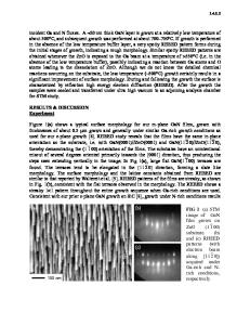
Molecular beam epitaxy growth utilising an RF-plasma nitrogen source was used to study surface reconstruction and surface morphology of GaN on GaAs (001) at 580 °C. While both the nitrogen flow and plasma excitation power were constant, the grown layers were characterised as a function of Ga-flux. In the initial growth stage a (3x3) surface reconstruction was observed. This surface periodicity only lasted up to a maximum thickness of 2.5 ML, followed by a transition to the unreconstructed surface. Samples grown under N-rich, Ga-rich and stoichiometric conditions were characterised by high-resolution scanning electron microscopy and atomic force microscopy. We found that the smoothest surfaces were provided by the N/Ga-ratio giving the thickest layer at the (3x3)=>(1x1) transition. The defect formation at the GaN/GaAs interface also depended on the N/ Ga-flux ratio.
1
Introduction
Gallium nitride is one of the most promising materials for optical applications in the blue range of the visible spectra due to its direct energy band gap of 3.39 eV at room temperature. The optical emission range of the GaN-based alloys can cover the whole visible range from near infrared to ultraviolet. Therefore much attention has been paid to these systems during the recent years. Heteroepitaxial layers, in the form of the thermodynamically stable hexagonal wurtzite crystal structure have mainly been grown by metal-organic vapor phase epitaxy (MOVPE) [1] [2]. The GaN can also be grown in the cubic (zinc blende) crystal structure [3], which is the usual form of other III-V compound semiconductors. However, the cubic nitrides are less stable than the hexagonal ones. The lack of a suitable lattice-matched substrate for high-temperature growth results in reduced GaN crystal quality. The most commonly used substrate is sapphire, where the lattice-mismatch is as large as 14%, and hexagonal GaN is obtained. The growth of the metastable cubic phase is unfavourable under equilibrium growth conditions such as MOVPE. The molecular beam epitaxy (MBE) technique provides the required nonequilibrium conditions at low growth temperatures. One advantage of MBE-growth on GaAs is the surface control given by reflection high-energy electron diffraction (RHEED) [3] and the know-how of cubic sub-
strates. The cubic GaAs and Si substrates have a large lattice-mismatch. The detailed conditions for MBE growth of layers with good structural quality are still not well known [4] [5]. A near-stoichiometric growth [5], or even slightly Ga-rich conditions [6] have been found to be important since the surface reconstruction of GaN on GaAs (001) depended on the N/Ga-ratio [7] [8] [9] [10]. When switching from N-rich to Ga-rich conditions, the surface ordering changed from (1x1) to c(2x2)