The Recrystallization Depth Control of the Excimer-Laser-Recrystallized Poly-Crystalline Silicon Film
- PDF / 1,343,295 Bytes
- 5 Pages / 384.12 x 617.04 pts Page_size
- 37 Downloads / 266 Views
ABSTRACT A novel method to control the recrystallization depth of amorphous silicon (a-Si) film during the excimer laser annealing (ELA) is proposed in order to preserve a-Si that is useful for fabrication of poly-Si TFT with a-Si offset in the channel. A XeCl excimer laser beam is irradiated on a triple film structure of a-Si/ thin native silicon oxide (-20A)/ thick a-Si layer. Only the upper a-Si film is recrystallized by the laser beam irradiation, whereas the lower thick a-Si film remains amorphous because the thin native silicon oxide layer stops the grain growth of the poly-crystalline silicon (poly-Si). So that the thin oxide film sharply divides the upper poly-Si from the lower a-Si.
INTRODUCTION Polycrystalline silicon thin film transistor (poly-Si TFT) is a promising device for active matrix liquid crystal display (AMLCD) due to superior current driving capability. However, poly-Si TFT has several critical problems such as large leakage current and long-term instability. In order to reduce the leakage current, various methods have been investigated such as offset gate [1] and lightly doped drain (LDD) [2]. Poly-Si TFT employing partial a-Si channel region near source and drain was reported to be quite effective in reducing the leakage current [3, 4]. The insertion of a-Si in the channel of poly-Si TFT requires additional deposition
and photolithography steps. The purpose of this new method is to preserve a-Si intentionally by precise recrystallization depth control during the excimer laser annealing of a-Si. The proposed method makes it possible to decide the location of the boundary between a-Si and poly-Si and does not require additional photolithography process. The new method allows large process margin in the fabrication of poly-Si TFT with uniform device characteristics in large area applications.
EXPERIMENT The process sequence of the proposed method is shown in Fig. 1. a-Si films of various thickness (800A, 2500A, 4000A) were deposited on the wet oxidized silicon wafer substrate by low pressure chemical vapor deposition (LPCVD) at 550'C or by plasma enhanced chemical vapor deposition (PECVD) at 300'C. Then the upper surface of a-Si was oxidized for 10 minutes in the cleaning solution of sulfuric acid (97% purity) and hydrogen peroxide (35% purity) with the volume ratio of 2:1 at 120'C. The thickness of the native silicon oxide film grown during the cleaning process was about 20 A, which was measured by transmission electron microscopy (TEM). On the oxidized a-Si, 400A thick a-Si film was deposited again by LPCVD or PECVD respectively. PECVD a-Si film was dehydrogenated at 450A in N2 ambient
689 Mat. Res. Soc. Symp. Proc. Vol. 557 © 1999 Materials Research Society
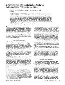
.... Native oxide
-
(a)
XeCI Excimner Laser Irradiation oys
a-Si
a-Si
.. Native o id
(b) Fig. 1 The process sequence of the proposed method. (a) Native oxide is grown by dipping in the solution of H 20 2 and H2SO4 at 120 for 10 minutes. (b) a-Si (400 A)/ thin native silicon oxide (-20A)/thick a-Si (800 A, 2500 A, 4000 A) stru
Data Loading...