Thin film backside gettering in n -type (100) Czochralski silicon during simulated CMOS process cycles
- PDF / 5,972,266 Bytes
- 11 Pages / 593.28 x 841.68 pts Page_size
- 44 Downloads / 278 Views
M. Tilli Laboratory of Physical Metallurgy, Helsinki University of Technology, 02150 Espoo, Finland
S. Hahn Siltec Silicon, 190 Independence Drive, Menlo Park, California 94025
C-C. D. Wong Integrated Device Technology, Inc., 3236 Independence Drive, Santa Clara, California 95051
F. A. Ponce Xerox Palo Alto Research Center, 3333 Coyote Hill Road, Palo Alto, California 94303 (Received 20 June 1988; accepted 3 January 1989)
The gettering effectiveness of various backside gettered polysilicon, silicon nitride, or poly + nitride film structures on n-type (100) Czochralski silicon wafers from a single ingot during simulated complementary-metal-oxide-semiconductor process cycles has been investigated by synchrotron section topography, breakdown voltage of 25-nm gate oxide, and minority carrier lifetime measurements. Interfacial structure was studied by cross-section transmission electron microscopy. Our studies show that for successful implementation of thin film backside gettering, good control of interactions between intrinsic gettering and thin film backside gettering during device processing cycles is critical. Thin film deposition generally increases oxygen precipitation. No extended defects propagate toward the bulk silicon. The structural and electrical quality of a denuded zone is found important. The best device yield (90%) is observed from the middle section wafers (with a 2 fim thick polysilicon backsurface coverage) which develop no recognizable bulk precipitates and stacking faults after the complete thermal cycles.
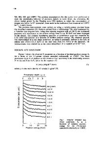
I. INTRODUCTION One of the extrinsic gettering (EG) methods for gettering metal impurities in silicon wafers is the deposition of a thin film layer of polysilicon on the wafer backsurface.1'2 Even though polysilicon thin film gettering is currently being used in actual device fabrication, its gettering mechanism is not well understood. Recently, we have reported the effects of polysilicon, silicon nitride, and poly + nitride backside gettering on ra-type (100) wafers and suggested that the polysilicon layer serves as an excellent sink for silicon interstitials and enhances the bulk oxygen precipitation.3 In this paper, the effects of polysilicon thickness on the thin film backside gettering efficiency of n-type (100) wafers with various oxygen levels from a single ingot during simulated complementary-metal-oxide-semiconductor (CMOS) process cycles were studied. The gettering efficiency was characterized by minority carrier lifetime and gate oxide breakdown voltage measurements. Extrinsic gettering (EG)-intrinsic gettering (IG) interactions were examined in terms of strain associated with bulk oxygen precipitation given by synchrotron section topography. Synchrotron section topography has proved a powerful nondestructive method for the study of defect distribution J. Mater. Res., Vol. 4, No. 3, May/Jun 1989
http://journals.cambridge.org
Downloaded: 19 Mar 2015
in semiconductor wafers. It has already been employed in the measurement of the denuded zone width in annealed silicon4'5 and in th
Data Loading...