Rapid Electrical Sintering of Nanoparticle Stuctures
- PDF / 1,982,960 Bytes
- 6 Pages / 612 x 792 pts (letter) Page_size
- 90 Downloads / 319 Views
1113-F02-07
Rapid Electrical Sintering of Nanoparticle Stuctures Ari T. Alastalo*, Tomi Mattila*, Mark L. Allen, Mikko J. Aronniemi, Jaakko H. Leppäniemi, Kimmo A. Ojanperä, Mika P. Suhonen and Heikki Seppä VTT Technical Research Centre of Finland, Tietotie 3, Espoo, P.O. Box 1000, FI-02044 VTT, Finland ABSTRACT A method for rapid electrical sintering (RES) of nanoparticle structures on temperaturesensitive substrates is presented. For an inkjetted silver nanoparticle conductor, a conductance increase of five orders of magnitude is demonstrated to occur in a timescale that typically varies between a few and one hundred milliseconds depending on process parameters. Furthermore, most of the conductance change takes only a few microseconds. The achievable final conductivities are within a factor of two from the bulk silver conductivity, as calculated using the external geometric dimensions of the structure ignoring porosity. The method is also applicable to other inorganic conductors such as indium-tin-oxide (ITO). More generally, the method offers a versatile tool in nanotechnology for electrical functionalization of nanoparticle structures. The method is also potentially suited for mass production. INTRODUCTION Inorganic materials are gaining a significant role in printed electronics. Silver nanoparticle- and flake-based inks for realizing conductor structures are widely available from companies such as Acheson, Parelec, Cabot, Advanced Nano Products (ANP), InkTec, and NanoMas . Conducting and semiconducting metal oxide dispersions have been increasingly studied for transparent-conductor (ITO), solar-cell (CIGS) [1] and transistor applications (Si, ZnO) [2,3,4] with many advantageous properties such as electrical performance and environmental stability over the organic counterparts [5]. Curing at elevated temperatures is a necessary step to form a functional, continuous structure of the deposited inorganic particles, especially for nanoparticle-based inks. Although the typical required sintering temperatures (150°C…250°C ) for the silver inks are only a fraction of the bulk material melting point (960°C) [6], they still limit the choice of the compatible paper or plastic substrates. Furthermore, the curing becomes even more challenging for metal oxide systems with higher melting points. To overcome the challenges of high-temperature curing, we present the rapid electrical sintering method (RES) for nanoparticle structures [7,8]. One of the key merits of the method is that the sintering process is induced locally in the nanoparticle structure, thus significantly reducing the thermal loading of the substrate [7]. The electrical sintering method is an alternative to conventional thermal (oven) sintering, as well as to laser sintering [9], photonic sintering [10] and microwave sintering [11].
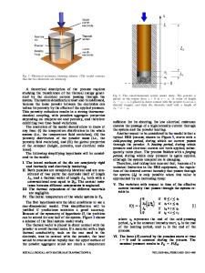
An example of the electrical sintering process is schematically shown in Figure 1. Here a conductor track with resistance Rtr is first printed on a substrate. Next, a voltage U is coupled between the contacting electrodes. A suff
Data Loading...