Realization of silicon nanopillar arrays with controllable sidewall profiles by holography lithography and a novel singl
- PDF / 1,864,680 Bytes
- 11 Pages / 612 x 792 pts (letter) Page_size
- 122 Downloads / 335 Views
1258-Q14-02
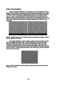
Realization of silicon nanopillar arrays with controllable sidewall profiles by holography lithography and a novel single-step deep reactive ion etching Yung-Jr Hung1,*, San-Liang Lee1, Brian J. Thibeault2 and Larry A. Coldren2 1 Department of Electronic Engineering, National Taiwan University of Science and Technology, No. 43, Sec. 4, Keelung Rd., Taipei, 106, Taiwan 2 Department of Electrical and Computer Engineering, University of California at Santa Barbara, Santa Barbara, CA, 93117, U.S.A. * E-mail: [email protected] ABSTRACT A simple and efficient approach for fabricating silicon nanopillar arrays with a high aspect ratio and controllable sidewall profiles has been developed by using holographic lithography and a novel single-step deep reactive ion etching. During the etching process, scalloping of the sidewalls can be avoided while reserving the high mask selectivity and high etching rate. Besides, the sidewall angle of resultant patterns can be adjusted by tuning the composition of the gas mixture of single-step DRIE process. We further fabricate a tapered silicon nanopillar array and observe its photonic bandgap property. We believe that the good optical performance of this tapered silicon nanopillar array realized by the proposed approach shows the promising of this process for various applications.
INTRODUCTION Silicon nanopillar arrays have been extensively used in many emerging technologies including bio-medical sensing [1], chemical sensing [2], and electronic field emission [3] via a large surface-to-volume ratio, optical wave-guiding [4, 5] via photonic bandgap properties, field effect transistors [6] via sub-100-nm single-crystalline silicon features, and antireflection coating on silicon [7, 8] via a lower effective index. Except for bottom-growth techniques, a sequence of patterning and etching processes is usually required to realize nanostructures in semiconductors. For patterning, most of nanostructures are realized using electron-beam lithography, covering only a small area. The disadvantages of being time consuming and with very low throughput are also the shortcomings for this technique. Nanoimprint lithography shows potential to replicate patterns with high throughput. But the key concerns of overlay, defects, and template patterning will distort the profile of the resultant patterns and degrade its uniformity. On the other hand, holographic lithography is an attractive method for periodic pattern generation with high regularity over a large area. Holographic system only requires easy-attainable and relatively inexpensive optical components to generate uniform interference patterns without using any mask. For etching, numerous methods have been reported for attaining high-aspect-ratio nanostructures. However, most of them require a metal hard mask formed mostly by lift-off process for the following deep etching [9-12]. This addition lift-off step will degrade the resolution of the profile and increase process complexity. Recently, self-masked dry etching technique is
Data Loading...