Resist Requirements and Limitations for Nanoscale Electron-Beam Patterning
- PDF / 881,675 Bytes
- 12 Pages / 612 x 792 pts (letter) Page_size
- 87 Downloads / 335 Views
H1.5.1
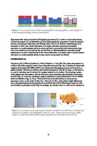
Resist Requirements and Limitations for Nanoscale Electron-Beam Patterning J. Alexander Liddle,1 Gregg M. Gallatin2 and Leonidas E. Ocola3 1 Materials Sciences Division, Lawrence Berkeley National Laboratory Berkeley, CA 94720, USA 2 IBM T.J. Watson Research Center Yorktown Heights, N.Y. 10598, USA 3 Advanced Photon Source, Argonne National Laboratory Argonne, IL 60439, USA ABSTRACT Electron beam lithography still represents the most effective way to pattern materials at the nanoscale, especially in the case of structures, which are not indefinitely repeating a simple motif. The success of e-beam lithography depends on the availability of suitable resists. There is a substantial variety of resist materials, from PMMA to calixarenes, to choose from to achieve high resolution in electron-beam lithography. However, these materials suffer from the limitation of poor sensitivity and poor contrast. In both direct-write and projection e-beam systems the maximum beam current for a given resolution is limited by space-charge effects. In order to make the most efficient use of the available current, the resist must be as sensitive as possible. This leads, naturally, to the use of chemically amplified (CA) systems. Unfortunately, in the quest for ever smaller feature sizes and higher throughputs, even chemically amplified materials are limited: ultimately, sensitivity and resolution are not independent. Current resists already operate in the regime of < 1 electron/nm2. In this situation detailed models are the only way to understand material performance and limits. Resist requirements, including sensitivity, etch selectivity, environmental stability, outgassing, and line-edge roughness as they pertain to, high-voltage (100 kV) direct write and projection electron-beam exposure systems are described. Experimental results obtained on CA resists in the SCALPEL® exposure system are presented and the fundamental sensitivity limits of CA and conventional materials in terms of shot-noise and resolution limits in terms of electron-beam solid interactions are discussed. INTRODUCTION Some years ago it was still possible to treat the resist requirements for high sensitivity and high resolution as two separate cases, divided between commercial applications, such as mask making, and small scale patterning for research. More recently, however, the separation between these two domains has all but disappeared. This has been driven primarily by the continuing reduction in feature size accompanying the progress of the semiconductor industry (Figure 1). The concomitant demands on mask fabrication have become rigorous, particularly with the introduction of sub-resolution elements for optical proximity effect correction [1]. In addition, as optical lithography becomes more difficult and costly, there is a strong possibility that electron-beam systems will be used directly [2, 3] for the mass production of integrated circuits (IC’s). These factors mean that electron-beam resists are now required to provide high resolution and high speed sim
Data Loading...