Simulation of Electron Beam Exposure and Resist Processing for Nano-Patterning
Electron beam lithography simulation is a powerful tool for the prediction of the resist profile after a complete lithographic process and the process optimization towards ultimate resolution and increased process latitude. In this chapter the structure o
- PDF / 2,554,789 Bytes
- 49 Pages / 439.37 x 666.142 pts Page_size
- 54 Downloads / 274 Views
Simulation of Electron Beam Exposure and Resist Processing for Nano-Patterning Ioannis Raptis and George P. Patsis
Abstract
Electron beam lithography simulation is a powerful tool for the prediction of the resist profile after a complete lithographic process and the process optimization towards ultimate resolution and increased process latitude. In this chapter the structure of such a simulation tool is presented and all core modules are explained in detail along with all major approaches developed for each of them (exposure, development, thermal treatment). Finally, two particular examples are given from simulation of complex patterns in the deep sub100 nm regime along with experimental data that confirm the accuracy and capabilities of the modern simulation tools.
3.1
Introduction
Electron beam lithography (EBL) is a very powerful lithographic technology able to resolve in a repeatable and reliable way, sub-10 nm patterns over large areas. Even though several other methodologies have been developed offering the same performance, EBL remains the choice for mask making applications and for prototyping. EBL is also used in the production of particular components such as Read-Write hard disk heads and is considered as a competitor for the next generation of ASIC’s and Multi Project Wafers, replacing optical lithography. Even though EBL has been around for decades, with the first vector scan tool developed by IBM at the early 70s, EBL tools are very expensive and their writing speed is still low or moderate if patterning very fine complex and dense structures. For those
I. Raptis (*) Institute of Microelectronics, NCSR “Demokritos”, Athens, Greece e-mail: [email protected] G.P. Patsis Department of Electronics, TEI of Athens, Athens, Greece M. Stepanova and S. Dew (eds.), Nanofabrication, DOI 10.1007/978-3-7091-0424-8_3, # Springer-Verlag/Wien 2012
43
44
I. Raptis and G.P. Patsis
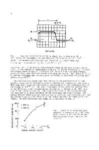
reasons, EBL machine time is in great demand and process optimization turnaround time should be minimized in order to decrease the overall cost. EBL is quite complicated, and includes several physical and chemical processing steps: electron beam – matter interaction, thermal processing steps (in the Chemically Amplified resists) and resist development. In order to decrease the process optimization time and cost, fast and accurate holistic simulation tools are needed based on accurate physical and chemical models describing all phenomena taking place during the various processing steps. Simulation outcomes should be multi-dimensional with detailed and accurate 3D information on resist profile, actual feature dimension and Line Edge Roughness (LER). Pattern dimension and LER define at a great percentage the device electrical characteristics and the overall IC size. All simulation features described above are common for all lithographic technologies. Additionally in EBL, the proximity effect sets significant obstacles in the realization of very fine and dense features. Proximity effect is the unwanted re-exposure of the resist
Data Loading...