Silicided P-N Junction Diodes Fabricated by Silicidation Through Silicon Buffer Layer and Dopant Drive-Out Process
- PDF / 323,378 Bytes
- 5 Pages / 414.72 x 648 pts Page_size
- 18 Downloads / 249 Views
47 Mat. Res. Soc. Symp. Proc. Vol. 320. ©1994 Materials Research Society
ox
oCosi2 0 oly Si
Co Si2
ox
ox
Si substrate
Si substrate
OX
ox
CoSi2 Si substrate
(b)
(a)
(c)
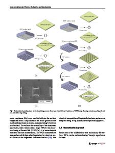
Fig.1 Schematic of the three types of diodes studied : (a) buffer silicon layer is partially consumed after silicidation; (b) buffer silicon layer is completely consumed after silicidation; and (c) no buffer silicon is used The diodes were implanted with BF 2 at beam energy 20 KeV and dosage 5x I015 cm- 2 . Almost all the dopants are contained within the top 600A in silicide as confirmed by secondary ion mass spectroscopy (SIMS). Dopant drive-out anneals at 900°C/60s and 1000°C/60s were performed to form p-n junctions. The I-V characteristics of these diodes were measured at 25-200'C, sheet resistance Rs was measured using four-point probe, and SIMS was performed by using Cs÷ as primary bombarding species. RESULTS AND DISCUSSION The thermal stability of CoSi 2 was studied by testing the sheet resistance of unpattemed film structures using four-point probe (Fig. 2).
2.6
2000 A amorphized polysilicon 2000 polysilicon :3U2000 A amorphous Si Si l00,,amorphous 0 ............... I"0A polysilicon 1000 A amorphized polysilicon --
........
w 2.4 -
..
2.2
A... 1.8 1.6
1.4 as-implanted
1st 900c/60s
Anneal
2nd 900c/60s
IOOOc/60s
sequence
Fig.2 Sheet resistance measurement during the thermal stability test. It is interesting to note that the sheet resistances do not increase even after two 900'C and one 1000'C rapid thermal anneals for a total time of 180 s. We have reported earlier that CoSi2/polysilicon /oxide structure degrades seriously under 900'C rapid thermal anneal for annealing time longer than 5 s [4, 5]. It is suspected that the microstructure of the polysilicon in CoSi 2 /polysilicon/Si structure evolves differently from the polysilicon in CoSi 2/polysilicon/SiO2 under rapid thermal anneals so the degradation is much less in the former structure. However the sheet resistance measurement does not seem to be sensitive
48
enough to predict diode electrical characteristics. Fig. 3 shows the leakage current density at -5 V for various types of diodes studied. 10 4 "-Ei-
11000'C buffered 900'C buffered 1000'C control
-
900'C control
10 3
102
S10 S100 14
control diodes on the same wafer, layer is etcheqt away 1ýy RIE C>
Ibuffyr
0
-
Buffer silicon categories Fig.3 Leakage current density of various diode of the area lx I0-3 cm 2 .The category indicates the thickness and microstructure of the buffer layers: poly2000 is 2000 A polysilicon; a-p2000 is 1000k amorphized polysilicon+ IOOOA polysilicon, alfa 2000 is 2000 A amorphous Si; polylOO0 is 1000A polysilicon; a-plOOO is 1000A amorphized polysilicon, and alfalO0O is 1000A amorphous Si. Also shown are the control diodes that have no buffer silicon layer and fabricated on the same chip. No significant difference in leakage current was observed for polysilicon, amorphized polysilicon, and amorphous Si samples with the same annealing temperature and same buffer layer thick
Data Loading...