Suppression of Parasitic BJT Action in Single Pocket Thin Film Deep Sub-Micron SOI MOSFETs.
- PDF / 127,262 Bytes
- 6 Pages / 612 x 792 pts (letter) Page_size
- 104 Downloads / 282 Views
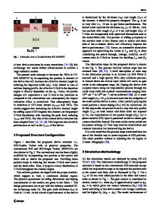
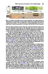
Suppression of Parasitic BJT Action in Single Pocket Thin Film Deep Sub-Micron SOI MOSFETs. Najeeb-ud-Din, Aatish K., Mohan V.Dunga, V. Ramgopal Rao and J.Vasi Electrical Engineering Department Indian Institute of Technology, Bombay, Powai, Mumbai - 400 076, INDIA ABSTRACT A study of parasitic bipolar junction transistor effects in single pocket thin film siliconon-insulators (SOI) nMOSFETs has been carried out. Characterization and simulation results show that parasitic bipolar junction transistor action is reduced in single pocket SOI MOSFETs in comparison to homogeneously doped conventional SOI MOSFETs. A novel Gate-InducedDrain-Leakage (GIDL) current technique was used to characterize the SOI MOSFETs. 2 - D simulations were carried out to analyze the reduced parasitic bipolar junction effect in single pocket thin film SOI MOSFETs. INTRODUCTION The advantages of SOI MOSFETs over their bulk counterparts are: simple dielectric isolation, increased circuit speed, elimination of latch up, reduced short channel effects and lower Hot Carrier Effects (HCE) [1]. The SOI technology has also shown great potential for mixed mode and analog applications [2]. However, the presence of buried oxide beneath the silicon film leads to floating body effects [3]. These floating body effects are detrimental to the operation of MOSFETs particularly in mixed mode/analog applications. The high drain field in deep sub-micron devices causes the impact ionization. The electrons move towards the drain, whereas holes move towards the film body region where they get accumulated. The floating body effect can give rise to kink and parasitic bipolar junction transistor (pBJT) action. The kink should be avoided but is not harmful in digital operation. The pBJT effect is detrimental especially in mixed mode analog/digital applications. Hence it needs to be constrained. Thin film SOI MOSFETs do not show the kink, but their circuit performance is severely restricted by the pBJT effect. In long channel devices, the holes recombine before reaching the source, whereas in short channel devices the hole current gets amplified by the BJT gain β, which depends on the base width (channel length). This amplified current gets added to the drain current. The major problems due to lateral bipolar gain are the parasitic BJT induced latch-up [4] and lowering of breakdown voltage [5]. Channel engineering has been successfully used to overcome some of the undesired effects in the MOSFET’s. Symmetric halo implantations are widely used in the bulk technology for the improvement of Short Channel Effects (SCE) and HCE [6]. Recently, asymmetric channel implantation at the source end has been introduced for bulk [7,8] MOSFETs. These Single Pocket (SP) devices show an improvement in the device performance like reduction in Drain Induced Barrier Lowering (DIBL) and threshold voltage (Vth) roll-off. The advantages of bulk asymmetric device for mixed mode applications have also been recently reported [9]. The SP implantation has also been introduced in the SOI technology [10
Data Loading...