The p-channel a-Si:H Thin Film Transistor with Plasma Etched Copper Electrodes
- PDF / 117,870 Bytes
- 6 Pages / 612 x 792 pts (letter) Page_size
- 3 Downloads / 283 Views
A4.12.1
The p-channel a-Si:H Thin Film Transistor with Plasma Etched Copper Electrodes
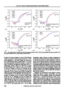
Helinda Nominanda, Guojun Liu, Hyun Ho Lee, and Yue Kuo Thin Film Nano and Microelectronics Research Laboratory, Department of Chemical Engineering, Texas A&M University, College Station, TX 77843-3122 ABSTRACT P-channel thin film transistors (TFTs) with a copper (Cu) gate, source, and drain electrodes, prepared by a novel plasma etching process, have been fabricated and studied. The p-channel TFT characteristics are similar to those of the p-channel TFT with Mo electrodes. The influence of the channel length on the TFT characteristics, such as mobility, threshold voltage, and on-off current ratio, was examined. In spite of its low mobility, good device characteristics, such as ohmic contacts, were obtained. Most of the TFT characteristics, except the threshold voltage, were not affected by an extended hightemperature annealing step. The increase of the threshold voltage was probably due to the lack of a diffusion barrier between the gate Cu and the gate SiNx layer. INTRODUCTION Conventionally, hydrogenated amorphous silicon thin film transistors (a-Si:H TFTs) are n-channel field-effect transistors (FETs). If p-channel a-Si:H TFTs were available, a complementary metal oxide semiconductor (CMOS)-type of circuit could be fabricated for various low-speed applications, such as sensors or detectors. P-type a-Si:H film properties, such as conductivity, are related to the deposition parameters and the substrate material [1,2]. In addition, TFT characteristics, such as threshold voltage and field effect mobility, are a function of the channel doping efficiency [1,3]. Refractory metal, such as molybdenum (Mo), secure the stable gate and source drain electrodes contact [4]. However, the use of a low-resistivity metal such as copper (Cu) is essential to large-area, high-density TFT array applications. Chemical mechanical polishing (CMP) is widely used to define the Cu lines [5]. CMP, however, is a complicated and costly process that is not compatible with large-area TFT array fabrication challenges. As an alternative, a novel plasma-based Cu etching process has been developed [6]. The process is composed of two simple steps: (1) the exposure of the photoresist-patterned Cu film to a Cl- or Brcontaining plasma, which converts the Cu to a CuClx or CuBrx compound, and (2) the subsequent removal of the compound with a dilute HCl solution [6]. A vertical wall profile and a high Cu etch rate was obtained at room temperature [6]. The plasma reaction was carried out in a conventional parallel-plate reactor. In this experiment, the authors have studied the performance of the p-channel a-Si:H TFT with a Cu/titanium tungsten (TiW) gate, source, and drain electrodes prepared from the plasma-based etching technology. The characteristics of this Cu/TiW TFT were compared with the TFT utilizing Mo electrodes. Reliability of the TFT under the extended annealing condition was also investigated.
A4.12.2
EXPERIMENTAL The self-aligned, inverted staggered, t
Data Loading...


