Vertical MOSFET Devices Fabricated on 3C-SiC with High and Low Material Quality
- PDF / 186,327 Bytes
- 6 Pages / 612 x 792 pts (letter) Page_size
- 65 Downloads / 308 Views
0911-B13-03
Vertical MOSFET Devices Fabricated on 3C-SiC with High and Low Material Quality Adolf Schoner1, Mietek Bakowski1, Per Ericsson1, Helena Stromberg1, Hiroyuki Nagasawa2, and Masayuki Abe2 1 Acreo AB, Kista, SE-16440, Sweden 2 HOYA Corporation, Sagamihara, 229-1125, Japan
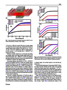
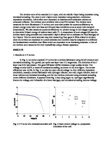
ABSTRACT Vertical DMOSFET devices with sizes from single cell to 1 mm2 large devices containing 960 unit cells have been fabricated on cubic 3C-SiC material. The used 3C-SiC substrates had varying material quality. The best quality had a more than 2 orders of magnitude lower density of extended crystal defects than the worst material. The processed and investigated vertical DMOSFET devices were designed for 600 V blocking voltage and had hexagonal unit cells with 2 µm channel length and aluminum implanted termination rings. The p-body was aluminum implanted and the source was phosphorus implanted. As deposited Ti/W contacts were evaluated as source and drain metallization. Single cell vertical DMOSFET devices processed on the low defect density material quality gave voltage blocking capabilities of more than 600 V with leakage currents of 0.1 to 10 µA. The same devices could handle currents around 5 mA in onstate at 15 V gate bias. MOSFET devices with up to 116 unit cells had blocking voltages of 400 to 500 V with on-state currents of 0.3 to 0.4 A at 15 V gate bias, indicating the potential of 3CSiC for the fabrication of next generation power MOSFET devices. INTRODUCTION 3C-SiC is a promising material for MOSFET devices to be used in medium power (600 1200 V, 10 – 100 A) applications, because of an expected high current handling capability due to a higher channel mobility compared to 4H-SiC. The so far poor performance of 4H-SiC MOSFETs is related to a large number of charge states at the SiO2/4H-SiC interface located in the band-gap close to the conduction band edge of 4H-SiC. These interface states limit the transport of electrons in the channel [1]. Due to the smaller bandgap of 3C-SiC, these electron transport limiting interface states are located in the conduction band and have therefore no effect on the transport properties of the channel. A higher channel mobility can be obtained and channel mobility values of 75 to 250 cm2/Vs have been reported for 3C-SiC [2-5]. In addition, a key commercial advantage of 3C-SiC is given by the usage of large diameter silicon substrates for the manufacturing of 3C-SiC wafers. 6” diameter 3C-SiC wafers have been demonstrated [6]. Large area substrates of good quality and the high channel mobility makes 3CSiC the material of choice for future medium voltage (600 - 1200 V) power MOSFETs. We have reported earlier on large area lateral and vertical 3C-SiC MOSFETs with varying size from a single unit cell to 3x3 mm2 [7-8]. Recently we reported on vertical DMOSFET devices with high current handling capability having channel mobilities of 30-50 cm2/Vs [9]. The high current handling was achieved by changing the ions for the source implantation from the
previously used nitrogen to phosphorus and by using
Data Loading...