Amorphous W-Zr Films as Diffusion Barriers Between Al and Si
- PDF / 871,782 Bytes
- 7 Pages / 417.6 x 639 pts Page_size
- 76 Downloads / 291 Views
. Res. Soc. Symp. Proc. Vol. 54. 1986 Materials Research Society
140
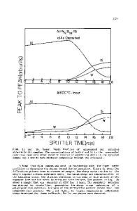
In this work, amorphous W-Zr alloy films are investigated as a diffusion The motivation for the selection of this barrier between Al and Si. particular pair of metals is derived from a previous work [11,17], where it is shown that an amorphous binary alloy that contains a near-noble element will tend to react by forming a near-noble metal silicide. We first establish that The main results of this study are twofold. interaction between an amorphous W-Zr alloy film and Al or Si occurs at temperatures much below the recrystallization temperature of the amorphous film. In addition, we examine the failure mode of a Si/W-Zr/Al contact structure and show that W-Zr is useful as a barrier between Al and Si only up to the temperature where Al starts to interact with the amorphous W-Zr film. EXPERIMENTAL PROCEDURE Substrates of -oriented n-type Si of 0.005 Qcm resistivity were used throughout this experiment to study the metallurgical interactions in the The crystallization of amorphous W-Zr /W-Zr and /W-Zr/Al systems. The deposition alloy films was investigated with samples of Al 0 /W-Zr. of amorphous W-Zr films was performed in an r.f. s~u~tering system equipped A magnetron-type circular with a diffusion pump and a cryogenic baffle. cathode, 3 in. in diameter, with a cathode-to-substrate spacing of 6 cm was To obtain W-Zr alloys with desired used as the sputtering source. compositions, a bare W (99.5%) cathode was partially covered with narrow Prior to loading into the sputtering system, the Si stripes of Zr (99.5%). substrates were first slightly oxidized in an oxygen plasma and then etched in The Al2 0 substrates were cleaned ultrasonically with a 1:10 HF for 2 min. The sputtering TCE, acetone and methanol and tRen blown dry with nitrogen. Torr be~fore chamber was evacuated to a base pressure of less than 1 x 10W-Zr films were sputter-deposited to a thickness of n800A to depoSition. Al depDsition was 1000A at a deposition rate of 400A/min in lOmTorr of Ar. Th• carried out without breaking vacuum, at a deposition rate of 120A/min. samples were then annealed in a vacuum furnace at pressures less than 5 x 10 Unless noted otherwise, all Torr in the temperature range of 400°C to 900°C. heat treatments lasted 30 min. Atomi 4 depth profiles and their evolution upon annealing were determined The phases of the reaction by 2 MeV He backscattering spectrometry (BS). products and the amorphous nature of the deposited films were established by SEM and EDAX were used to examine changes glancing angle x-ray diffraction. in surface morphologies of the samples after heat treatment. The n+p shallow junction for testing the performance of /W-Zr/Al contacts were prepared on oriented p-type Si of 10-20Qcm resistivity. After an initial wet oxide of 4500A was grown, three photolithographic steps The first were executed to fabricate the junctions and thý metallizations. mask defined the diflfision aYeas of 500 x 500 ]jm . The junctions were formed As/cm at 150 keV into the dif
Data Loading...