Carbon Doped Silicon Emitters Fabricated Using Limited Reaction Processing
- PDF / 315,436 Bytes
- 6 Pages / 420.48 x 639 pts Page_size
- 43 Downloads / 308 Views
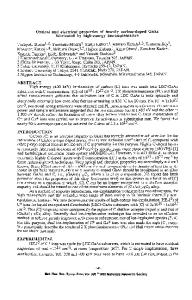
CARBON DOPED SILICON EMITTERS FABRICATED USING LIMITED REACTION PROCESSING F.H. RUDDELL, B.M. ARMSTRONG AND H.S; GAMBLE The Queen's The Institute of Advanced Microelectronics, University of Belfast, Ashby Building, Stranmillis Road, Belfast, BT9 5AH, Northern Ireland K.B. AFFOLTER, P.B. MOYNAGH AND P.J. ROSSER STC Technology Ltd., England ABSTRACT This paper describes the deposition of in-situ doped N-type silicon carbide layers in a Limited Reaction Processing (LRP) reactor. Silane/propane~phosphine gas chemistry was used at temperatures less than 1000 C and SIMS, XPS and TEM analysis techniques aided layer characterisation. A low thermal budget deposition process (1 min at 970 C) was employed to form the emitters of Sic/Si heterojunction NPN bipolar transistors. These devices yielded a factor of two increase in emitter Gummel number compared to diffused emitters. INTRODUCTION The future production of high gain/high speed bipolar transistors will be based on the use of heterojunction structures. Successful HBT's have been produced using GaAs/ GaAlAs structures, however there is at present a strong incentive to produce silicon-based heterostructures which could be incorporated into existing BiCMOS process schedules. Silicon carbide (SiC) has attracted interest for use as a wide bandgap emitter material. The bandgap of B-SiC is 2.2 eV and it exhibits high thermal stability, controllable conductivity and high electron saturated drift velocity [1]. However the temperature needed,6 for epitaxial growth of SiC on silicon can be as high as 1300 C. This is clearly unacceptable if the material is to be used as a replacement for polysilicon on a scaled device structure. In an LRP reactor fast wafer heating using tungstenhalogen lamps is combined with low pressure chemical vapour deposition technology. The deposition reaction is essentially controlled by temperature and so layer growth is determined by the applicati 8 n of power to the heating lamps. Heating rates of up to 200 C/s have been used to minimise process thermal budget. This paper describes the silicon carbide deposition process and then briefly discusses the performance of heterojunction emitters formed using the LRP-deposited material. SILICON CARBIDE DEPOSITION All the silicon carbide deposition work was carried out in the QUPLAS LRP reactor, already proven as an epitaxial silicon deposition system [2] (Fig. 1). The reactor consists of an evacuated quartz envelope in which the single process wafer is heated by 18_ý00 W tungsten-halogen lamps. A base pressure of less than 10 mbar is achieved using turbomolecular and rotary pumps. A microwave source is situated upstream of the wafer Mat. Res. Soc. Symp. Proc. Vol. 198. 01990 Materials Research Society
554
R.F. Generator 2.45 GHz
Loading Door
Quartz Tube _
+
Wafer +
Plasma
Inlet
Fig.
1.
-
Silicon +
Gas
[-
OOO
Quartz Boat
Tungsten-Halogen Heating Lamps
'U
I Vacuum Pump
Schematic cross-section of QUPLAS LRP reactor
position allowing an in-situ plasma pre-clean process to precede layer depositio
Data Loading...