Effect of GaAs Surface Treatments on Lanthanum Silicate High-K Dielectric Gate Stack Properties
- PDF / 145,303 Bytes
- 6 Pages / 612 x 792 pts (letter) Page_size
- 79 Downloads / 392 Views
1073-H06-04
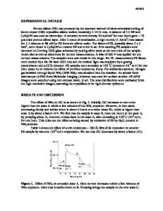
Effect of GaAs Surface Treatments on Lanthanum Silicate High-K Dielectric Gate Stack Properties Daniel J Lichtenwalner1, Rahul Suri2, and Veena Misra2 1 Materials Science and Engineering, North Carolina State University, 1001 Capability Drive, 214 Research Building 1, Raleigh, NC, 27695-7919 2 Electrical and Computer Engineering, North Carolina State University, Raleigh, NC, 276957920 ABSTRACT The properties of lanthanum silicate (LaSiOx) gate stacks on GaAs substrates have been examined, comparing different GaAs pretreatments; namely a) as-received, b) HCl-treated, and c) sulphur-treated. X-ray photoelectron spectroscopy of the As 3d, Ga 3d, and Ga 2p binding energy peaks were used to reveal the chemical nature of the stacks. After a 400 °C in situ anneal in 10-6 torr pO2, the LaSiOx chemically reduces the As oxides from the as-received GaAs, while Ga oxide species remain. HCl and S-treated GaAs similarly show no As oxides, and a much smaller degree of Ga oxides than the as-received case. The Ga-S bonding may be responsible for lowering the tendency towards Ga oxidation for the S-treated case. On p-type, Zn-doped GaAs, 3.0 nm lanthanum silicate films produce MOS device EOT values of 2.38 nm, 1.51 nm, and 1.37 nm, on as-received, HCl-treated, and S-treated substrates, respectively. The high EOT for the asreceived GaAs corresponds to the thicker Ga oxide and elemental As at the interface. The decreases in both Ga oxide and elemental As at the interface of the S-treated stack appears to be related to it having the lowest EOT devices.
INTRODUCTION In the effort to further enhance MOSFET scaling, alternative semiconductor channel materials are being investigated that have higher charge carrier mobility and velocity than Si. In particular, GaAs-based materials are under investigation as potential n-channel materials due to their high electron mobility. For implementation, an appropriate dielectric material is needed which provides good chemical compatibility, and the gate stack requires a proper effective work function for nMOSFET device optimization. Lanthanum silicate (LaSiOx) has been shown on silicon to achieve sub-nm EOT devices by reaction to eliminate interfacial silica layers [1], with relatively low gate leakage, having an amorphous phase stability up to 1000°C [2]. A key feature is that a LaSiOx gate stack on Si provides nMOSFET band-edge threshold voltages to be obtained with typically mid-gap electrodes, such as TaN [3]. The LaSiOx band gap and energy band offsets should be appropriate for GaAs as well [4]. These reasons make LaSiOx an interesting candidate for investigation as a gate dielectric for GaAs-based nMOSFETs. In this investigation, we examine the properties of LaSiOx formed by reactive evaporation in a UHV MBE system on GaAs. While one must consider many key property differences between GaAs and Si to fully characterize a given MOS stack structure on GaAs [5], the interface properties can be expected to be one major source of difference between these two cases, as the GaAs surface is
Data Loading...