Effective Dielectric Thickness Scaling for High-K Gate Dielectric Mosfets
- PDF / 118,139 Bytes
- 5 Pages / 612 x 792 pts (letter) Page_size
- 57 Downloads / 456 Views
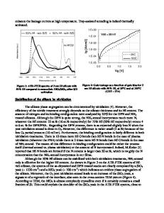
Effective dielectric thickness Scaling for High-K Gate Dielectric MOSFETs Krishna Kumar Bhuwalka, Nihar R. Mohapatra, Siva G. Narendra1, V Ramgopal Rao Electrical Engineering Department Indian Institute of Technology, Bombay 400 076, India. 1 Microprocessor Research Lab, Intel Corporation Hillsboro, OR, USA. ABSTRACT It has been shown recently that the short channel performance worsens for high-K dielectric MOSFETs as the physical thickness to the channel length ratio increases, even when the effective oxide thickness (EOT) is kept identical to that of SiO2. In this work we have systematically evaluated the effective dielectric thickness for different Kgate to achieve targeted threshold voltage (Vt), drain-induced barrier lowering (DIBL) and Ion/Ioff ratio for different technology generations down to 50 nm using 2-Dimensional process and device simulations. Our results clearly show that the oxide thickness scaling for high-K gate dielectrics and SiO2 follow different trends and the fringing field effects must be taken into account for estimation of effective dielectric thickness when SiO2 is replaced by a high-K dielectric. INTRODUCTION Continuous down scaling of CMOS devices into deep sub-micrometer dimensions seems to have reached its limits with SiO2 as the gate dielectric material [1]. Alternative high-K materials such as Al2O3 (K~10), HfO2/ZrO2 (K~25), La2O3 (K~27), TiO2 (K~60-100) have been suggested, which provide higher physical thickness (by a factor of TK/TSiO2) and reduce the direct tunneling leakage current. However, the higher physical thickness results in increased fringing fields from gate to the source/drain regions thereby degrading the gate control and sub-threshold performance [2]. For successful induction into the mainstream technology, the short channel performance of MOS transistors with high-K gate dielectrics must be comparable to the conventional SiO2 with identical effective oxide thickness (EOT). It is well established in the literature that the use of high-K dielectric leads to a degradation in device performance in terms of its short-channel behavior. The fringing fields from the gate to source/drain regions have been identified as responsible for this degradation [3,4]. In this work, we found that there is an increase in Drain-Induced-Barrier-Lowering (DIBL) and decrease in the threshold voltage (Vt) and Ion/Ioff ratio, with increase in K value, when the effective oxide thickness kept identical. To counter the effect of degradation in the short-channel performance with the use of high-K dielectrics, one needs to decrease the effective oxide thickness for high-K gate dielectrics below that of SiO2. This would mean that the gate oxide thickness needs to be scaled more aggressively with high-K dielectrics than predicted by the roadmap values for SiO2. Thus, we show for the first time using detailed two-dimensional (2-D) simulations that, in order to match SiO2 performance, the effective thickness of the gate dielectric is not the scaled EOT, as predicted by the ratio of their dielectric co
Data Loading...