Group III-Sb Metamorphic Buffer on Si for p-Channel all-III-V CMOS: Electrical Properties, Growth and Surface Defects
- PDF / 593,640 Bytes
- 6 Pages / 432 x 648 pts Page_size
- 77 Downloads / 290 Views
Group III-Sb Metamorphic Buffer on Si for p-Channel all-III-V CMOS: Electrical Properties, Growth and Surface Defects Shun Sasaki1,3, Shailesh Madisetti1, Vadim Tokranov1,Michael Yakimov1, Makoto Hirayama1, Steven Bentley2, Rohit Galatage2, Ajey P. Jacob2, and Serge Oktyabrsky1 1
SUNY College of Nanoscale Science and Engineering, Albany NY 12203, USA GLOBALFOUNDRIES at Albany NanoTech, Albany, NY 12203, USA 3 SUMCO Corporation, Minato-ku, Tokyo 105-8634, JAPAN 2
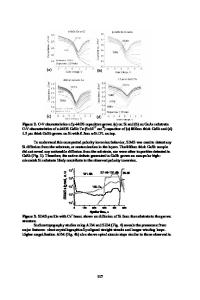
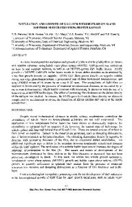
ABSTRACT Group III-Sb compound semiconductors are promising materials for future CMOS circuits. Especially, In1-xGaxSb is considered as a complimentary p-type channel material to n-type In1xGaxAs MOSFET due to the superior hole transport properties and similar chemical properties in III-Sb’s to those of InGaAs. The heteroepitaxial growth of In1-xGaxSb on Si substrate has significant advantage for volume fabrication of III-V ICs. However large lattice mismatch between InGaSb and Si results in many growth-related defects (micro twins, threading dislocations and antiphase domain boundaries); these defects also act as deep acceptor levels. Accordingly, unintentional doping in InGaSb films causes additional scattering, increase junction leakages and affects the interface properties. In this paper, we studied the correlations between of defects and hole carrier densities in GaSb and strained In1-xGaxSb quantum well layers by using various designs of metamorphic superlattice buffers. INTRODUCTION Group III-Sb compound semiconductors are promising materials for high-speed, low power electronic devices due to their superior hole and electron transport properties. So far, InGaAs and Ge have been extensively studied as silicon CMOS N & P respective replacement for sub 10nm technology node. However, GaSb and its ternary or quaternary compounds have been recently attracting much attention as p-type channel materials due to their superior hole mobility, large controllable band offsets for high-performance tunnel FETs, and similar chemical properties to those of InGaAs. Furthermore, In1-xGaxSb epitaxy on Si substrate would provide low cost device fabrication and the possibility of co-integration with existing silicon devices. Large lattice mismatch between III-Sb’s and Si generates structural defects such as micro twins, threading dislocations and antiphase domain boundaries [1]. These defects result in unintentional p-type doping, and some of them can pass through the surface. The antimonide-based compounds have highly reactive surfaces and tend to produce elemental Sb as the end product of reaction with oxygen in atmosphere [2]. These properties result in relatively poor surface quality and unintentional doping of InGaSb and thus preventing from realization of high performance In1-xGaxSb transistors. Interpretation and control of unintentional acceptor doping is essential for development of commercial III-Sb semiconductor products. We report on the relationships between the defects and various designs of metamorphic superlattice buffers on electrical properties of GaSb
Data Loading...