Textural Evolution of Cu Damascene Interconnects after Annealing
- PDF / 451,802 Bytes
- 6 Pages / 612 x 792 pts (letter) Page_size
- 99 Downloads / 415 Views
F8.9.1
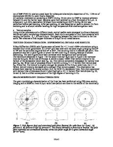
Textural Evolution of Cu Damascene Interconnects after Annealing Jae-Young Cho, Hyo-Jong Lee1, Hyoungbae Kim and Jerzy A. Szpunar Department of Mining, Metals and Materials Engineering, McGill University, Montreal, Quebec, H3A 2B2, Canada 1 School of Materials Science and Engineering and Research Institute of Advanced Materials, Seoul National University, Seoul 151-744, Korea ABSTRACT Textural evolution of Cu interconnects having a different line width was investigated after annealing. Texture was measured on the surface of Cu interconnects using EBSD (electron backscattered diffraction) techniques including GBCD (grain boundary character distribution). To analyze a relationship between the stress distribution and textural evolution in the samples investigated, the micro stresses were calculated for the different line width at 200°C using FEM (finite element modeling). In this investigation, it was found that the inhomogeneity of stress distribution in Cu interconnects is an important factor is necessary for understanding textural transformation after annealing. A new interpretation of textural evolution in damascene interconnects lines after annealing is suggested, based on the state of stress and the growth mechanisms of Cu electrodeposits. INTRODUCTION As the features of integrated circuitry (IC) chips are scaled down to submicron dimensions, the manufacturer demands new technology to meet performance and reliability requirements for the electronic interconnects. According to these technical demands, the copper damascene process became an important issue in the integrated circuitry (IC) chips industry since it allows a decrease in RC (resistance and capacitance) delay losses, reduces the number of processing operations and increases the lifetime of the interconnect lines [1]. Since the Cu damascene process has been introduced in the IC chips industry, significant research on the relationship between texture and reliability of copper interconnects has been undertaken. It is well known that strong {111} texture increases the resistance of electromigration failure and this failure can be correlated with the frequency of the occurrence of CSL (coincidence site lattice) boundaries or low or high diffusivity boundaries and the strength of {111} texture in aluminum thin films [2]. However, such relationship for the Cu hasn’t been firmly established and the driving forces which can affect the textural evolution during annealing were not clearly identified until now [35]. In this study, the details of textural evolution will be examined using electron backscattered diffraction (EBSD) techniques and the stress contribution to the evolution of texture and microstructure during annealing will be discussed. A model for the textural transformation as the line width decreases after annealing based on the state of stress and the growth mechanisms of Cu electrodeposits will be proposed. EXPERIMENTAL PROCEDURE Two different samples, one as-deposited and another annealed were used for this investigation. Both samples were f
Data Loading...